1. The Single-Layer Antireflection Coating
The simplest form of an antireflection coating is a single-layer coating. This method is often effective for reducing reflection loss from high-index substrates.
Basic Principle
Consider Figure 4.1, which illustrates a vector diagram. For a single-layer coating:
- Two vectors represent the amplitude reflection coefficients at the interfaces.
- If the incident medium is air, and the film index is lower than the substrate index, the reflection coefficients are negative due to a 180° phase change at each interface.
The resultant locus forms a circle, with a minimum reflectance at the wavelength where the layer has a quarter-wave optical thickness (\( \delta = 90^\circ \)).
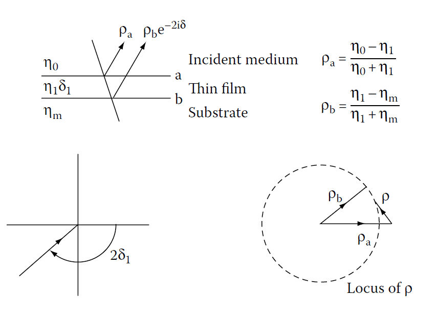
Vector diagram of a single-layer antireflection coating.
Condition for Zero Reflectance
Complete cancellation occurs if the two vectors are equal in length and opposite in direction. The condition is:
\[
y_0 – y_1 = y_1 – y_m
\]
Which simplifies to:
\[
y_1^2 = y_0 y_m
\tag{4.1}
\]
In terms of refractive indices at optical frequencies:
\[
n_1^2 = n_0 n_m
\]
At oblique incidence, the admittances \(( y )\) are replaced by tilted admittances \(( \eta )\).
Reflectance Equation
The optical admittance of a quarter-wave layer is:
\[
Y = \frac{y_1^2}{y_m}
\]
The reflectance (( R )) is:
\[
R = \left( \frac{y_0 – Y}{y_0 + Y} \right)^2 = \left( \frac{y_0 – \frac{y_1^2}{y_m}}{y_0 + \frac{y_1^2}{y_m}} \right)^2
\]
This reflects that perfect antireflection occurs when:
\[
y_1 = \sqrt{y_0 y_m}
\]
If there is a small error \(( \varepsilon )\) in \( y_1 \), such that:
\[
y_1 = (1 + \varepsilon) \sqrt{y_0 y_m}
\]
The residual reflectance is approximately:
\[
R \approx 4 \varepsilon^2
\]
A 10% error \(( \varepsilon = 0.1 )\) results in a residual reflectance of 1%.
Practical Applications
- Zinc sulfide (\( n = 2.2 \) at 2 µm and \( n = 2.15 \) at 15 µm) is widely used as a single-layer coating material for substrates like germanium, silicon, and other semiconductors.
- Substrates such as germanium (\( n = 4.0 \), reflection loss ≈ 36%) and silicon (\( n = 3.5 \), reflection loss ≈ 31%) require such coatings to reduce reflection losses to a few percent.
Deposition Techniques
- For durable zinc sulfide films, the substrate is maintained at around 150°C during coating, with glow discharge cleaning prior to deposition.
- Alternatives include cerium oxide (\( n = 2.2 \)) and silicon monoxide (\( n = 1.9 \)), which are harder and more robust.
Incidence Angle and Polarization Effects
At oblique incidence, the phase thickness decreases due to the cosine term:
\[
\delta = \frac{2 \pi n d \cos \vartheta}{\lambda}
\]
The optimum wavelength shifts shorter, and polarization effects become evident. However, these effects are smaller for high-index substrates.
Reflectance and Transmittance at Oblique Incidence
Using the matrix method, the characteristic matrix for a single film on a substrate is:
\[\begin{bmatrix} B \\ C \end{bmatrix} = \begin{bmatrix} \cos \delta & i \sin \delta / \eta_1 \\ i \eta_1 \sin \delta & \cos \delta \end{bmatrix} \begin{bmatrix} 1 \\ \eta_m \end{bmatrix} \]
Where:
\[
\delta = \frac{2 \pi n_1 d_1 \cos \vartheta}{\lambda}
\]
The amplitude reflection coefficient is:
\[
\rho = \frac{\eta_0 – \frac{B}{C}}{\eta_0 + \frac{B}{C}}
\]
The reflectance is:
\[
R = \left| \rho \right|^2
\]
Admittance Diagram
Figure 4.5 shows the admittance locus for a single-layer antireflection coating. For normal incidence:
- The locus is a circle, starting at \( Y = 4.0 \) (admittance of germanium).
- The circle intersects the real axis at \( Y = 2.22/4.0 = 1.21 \), corresponding to a quarter-wave thickness.
Figures
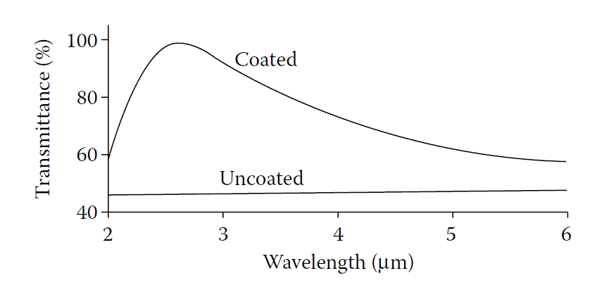
- Figure 4.2: Transmittance of a germanium plate with a single-layer zinc sulfide coating.
- Figure 4.3: Transmittance of a silicon plate with silicon monoxide coating.
- Figure 4.4: Variation of performance with incidence angle for zinc sulfide on germanium.
- Figure 4.5: Admittance diagram for a single-layer coating.
This analysis underscores the simplicity and effectiveness of single-layer antireflection coatings, especially for high-index substrates.
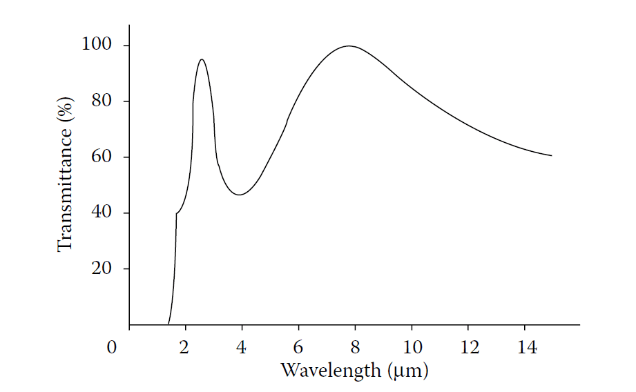
Transmittance of a germanium plate bloomed on both sides with zinc sulfide for 8 μm.
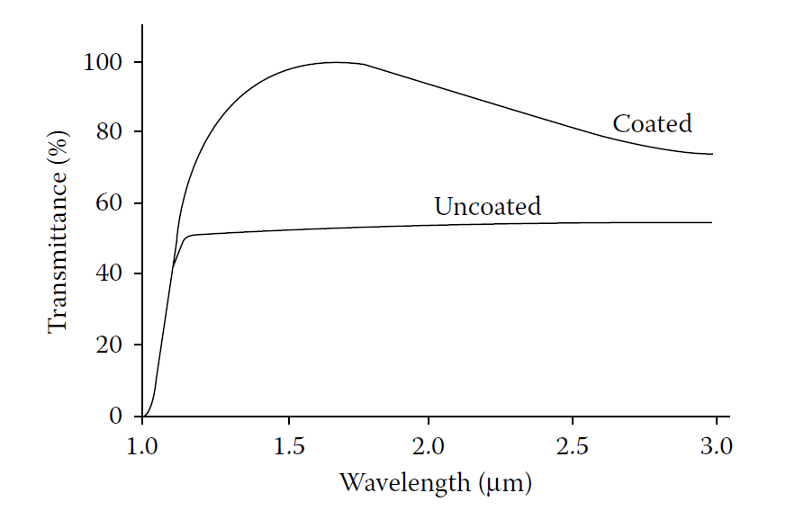
Transmittance of a 1.5-mm-thick silicon plate with and without antireflection coatings of silicon monoxide, a quarter-wavelength thick at 1.7μm.
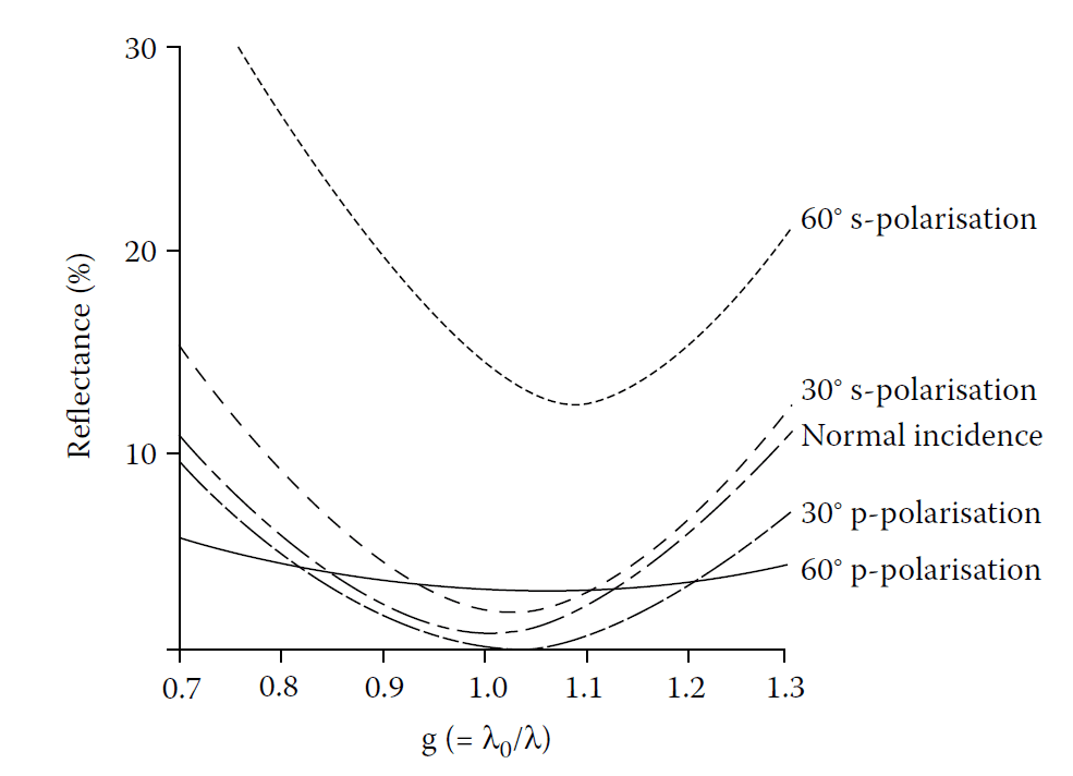
Calculated performance at various angles of incidence of a zinc sulfide coating (n=2.2) on a
germanium substrate (n=4.0).
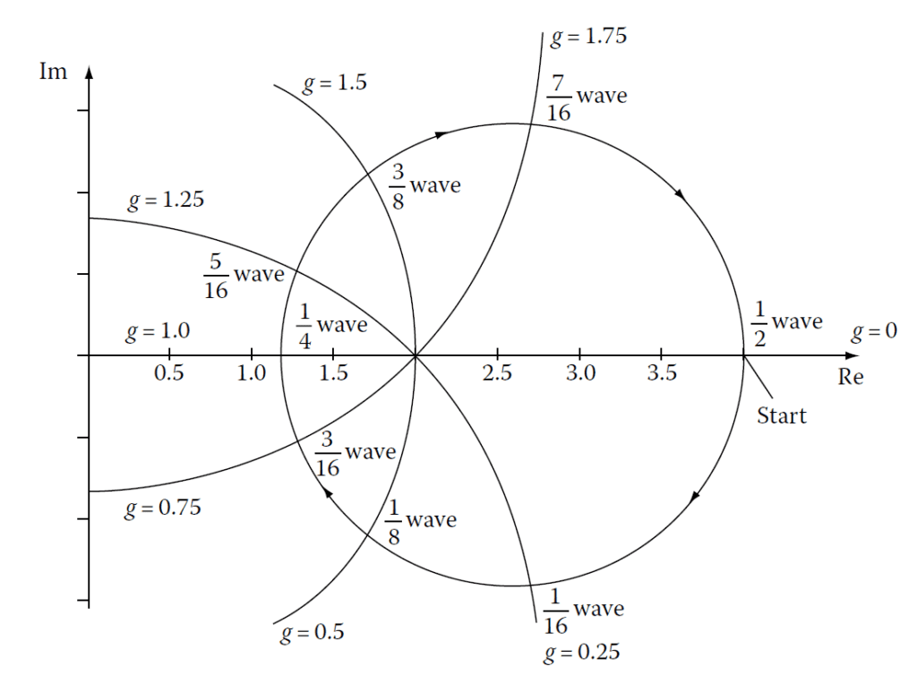
Admittance diagram for a single-layer zinc sulfide (n=2.2) coating on germanium (n=4.0).
2. Double-Layer Antireflection Coatings
Overview
Single-layer antireflection coatings are limited in their design flexibility and performance:
- The refractive index of the layer and its quarter-wave optical thickness are fixed parameters for achieving zero reflectance.
- These coatings achieve zero reflectance at only one wavelength and have narrowband performance.
Double-layer coatings introduce additional layers to overcome these limitations, providing:
- Flexibility in layer thickness design.
- Broader wavelength performance.
Principle of Double-Layer Design
For zero reflectance at a single wavelength using a two-layer system:
- The layers have indices lower than that of the substrate (\( n_m \)).
- The thicknesses of the two layers are adjusted to satisfy the required reflectance condition.
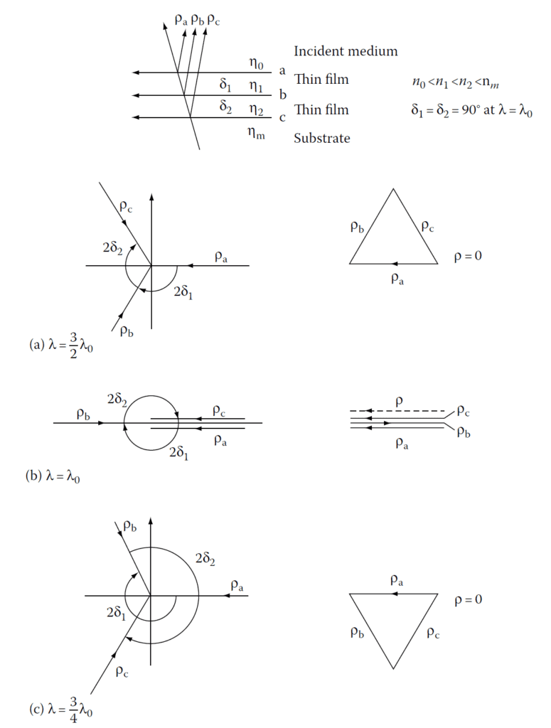
Vector Diagram Representation
Figure 4.6 shows a vector diagram for a two-layer coating:
- Two configurations of thickness are possible to achieve zero reflectance:
- Thinner combination (Figure 4.6a): Yields broader performance and is generally preferred.
- Thicker combination (not shown here): Offers similar results but is narrower in bandwidth.
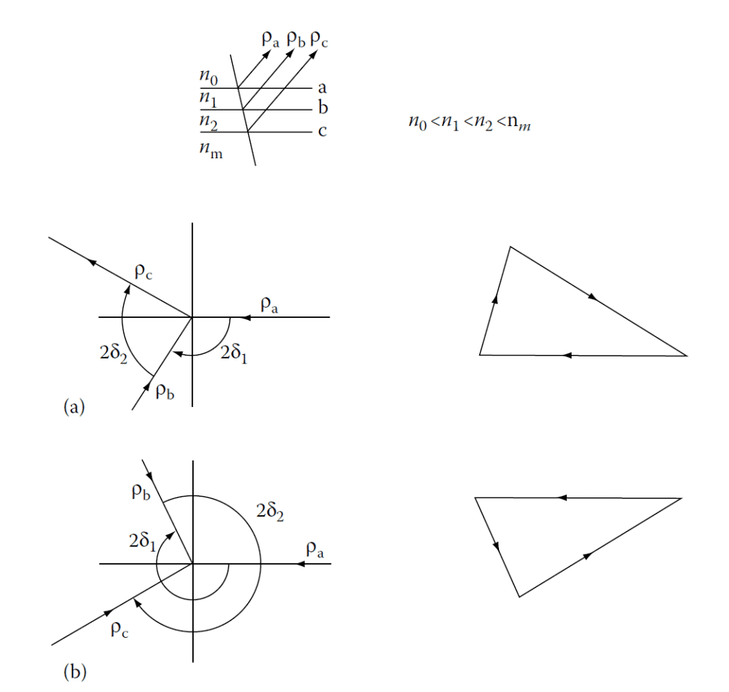
Vector diagram for double-layer antireflection coating. The thickness of the layers can be chosen
to close the vector triangle and give zero reflectance in two ways, (a) and (b).
Admittance Diagram Analysis
Figure 4.7 illustrates the design using an admittance diagram:
- Admittances are plotted in free space units (numerically equal to refractive indices).
- Intersection points of circles representing layer indices determine possible solutions.
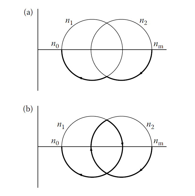
Admittance diagram for the double-layer antireflection coating. The two possible solutions are
shown in (a) and (b).
Mathematical Approach Using the Matrix Method
The characteristic matrix of a two-layer system is:
\[ \begin{bmatrix} B \\ C \end{bmatrix} = \begin{bmatrix} \cos \delta_1 & i \sin \delta_1 / y_1 \\ i y_1 \sin \delta_1 & \cos \delta_1 \end{bmatrix} \begin{bmatrix} \cos \delta_2 & i \sin \delta_2 / y_2 \\ i y_2 \sin \delta_2 & \cos \delta_2 \end{bmatrix} \begin{bmatrix} 1 \\ y_m \end{bmatrix} \]
For zero reflectance, the optical admittance at the interface must equal the admittance of the incident medium (\( y_0 \)):
\[
Y = y_0
\]
Expanding and separating real and imaginary parts gives the following system of equations:
- Real part:
\[
-y_m \sin \delta_1 \sin \delta_2 + y_0 y_2 \cos \delta_1 \cos \delta_2 + y_1 \cos \delta_1 \cos \delta_2 = 0
\] - Imaginary part:
\[
y_1 y_2 \sin \delta_1 \sin \delta_2 + y_0 y_m \cos \delta_1 \cos \delta_2 = y_0 y_1
\]
Conditions for Zero Reflectance
To simplify, these equations yield the following relationships between the layers’ phase thicknesses (\( \delta_1 \) and \( \delta_2 \)):
- Phase thickness relationship:
\[
\tan \delta_2 = \frac{(y_2 y_m – y_0 y_2)}{(y_0 y_1 – y_m y_1)}
\tag{4.4}
\] - Layer thickness relationship:
\[
\tan \delta_1 = \frac{(y_1 y_2 – y_0 y_m)}{(y_0 y_2 – y_1 y_m)}
\tag{4.5}
\] - General solution for ( \delta_1 ) and ( \delta_2 ):
\[
\tan^2 \delta_1 = \frac{(y_2 y_m – y_0 y_2)(y_1 y_m – y_0 y_1)}{(y_0 y_1 y_2 – y_m)^2}
\]
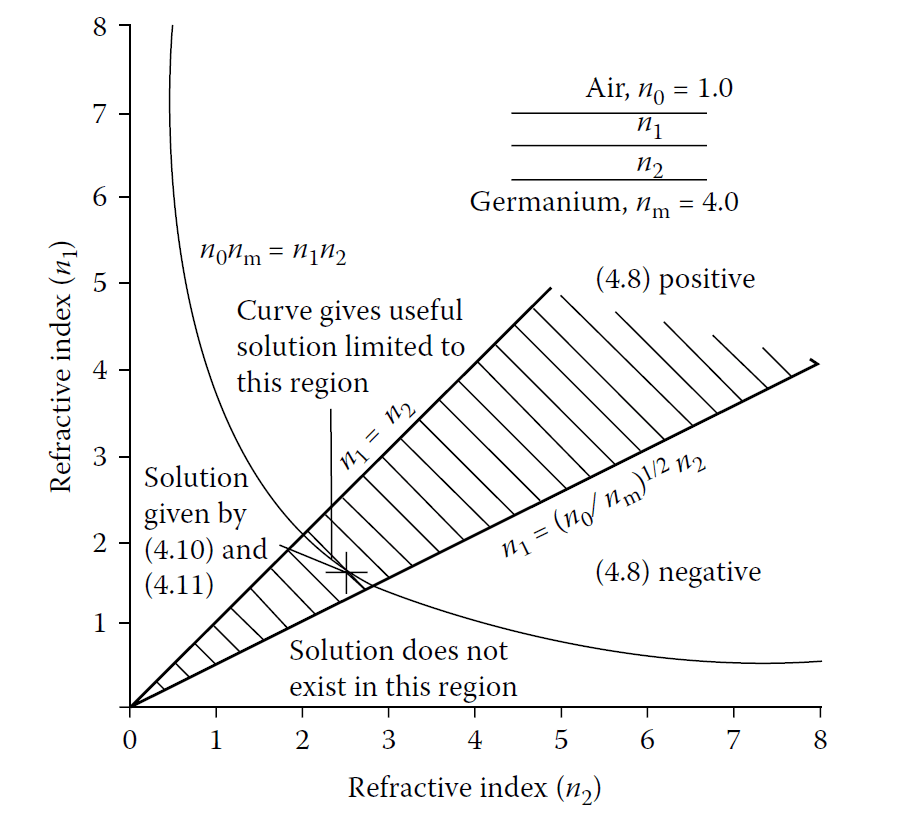
Schuster Diagram and Validity Conditions
For a valid solution:
- The intersection points in the admittance diagram must exist.
- The following conditions must be met (from Equations 4.7–4.9):
- \( (y_2 – y_0 y_m)^2 \geq 0 \)
- \( (y_1 y_m – y_0 y_2)^2 \geq 0 \)
- \( (y_0 y_1 – y_1 y_m)^2 \geq 0 \)
These conditions are summarized in the Schuster diagram (Figure 4.8).
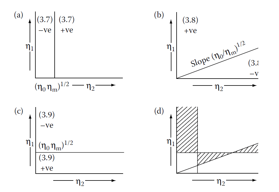
The construction of a Schuster diagram. (a), (b), and (c) are combined in one diagram in (d), and
the shaded areas are those in which real solutions exist.
Example: Double-Layer Coating on Germanium
For germanium (\( n_m = 4.0 \)) in air (\( n_0 = 1.0 \)):
- Layer 1: \( n_1 = 2.50 \)
- Layer 2: \( n_2 = 1.59 \)
- Reflectance at the reference wavelength \( \lambda_0 \): 5.6%.
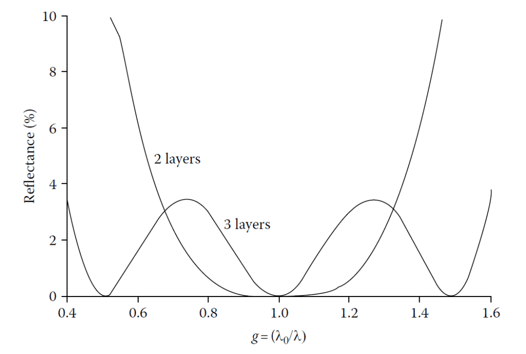
Theoretical performance curves for such coatings are shown in Figures 4.9–4.11.
Transmittance of a germanium plate with two-layer antireflection coatings of MgF2 (nd=λ/4 at
1.03μm) and germanium (nd=λ/4 at 0.61μm), the germanium being the outermost layer.
Vector diagrams for quarter-quarter antireflection coatings on a high-index substrate; (a), (b),
and (c) represent wavelengths of (3/2)λ\(_0\), λ\(_0\), and (3/4)λ\(_0\), respectively.
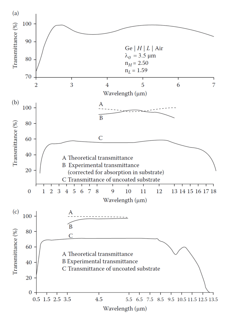
Double-layer antireflection coatings for high-index substrates. (a) Theoretical transmittance
of a quarter-quarter coating on germanium (single surface). (b) Theoretical and measured
transmittance of a similar coating on arsenic trisulfide glass (double surface). (c) Theoretical
and measured transmittance of a similar coating on arsenic triselenide glass (double surface).
Special Case: Equal Thickness Layers
When both layers have equal optical thicknesses (\( \delta_1 = \delta_2 = \delta \)):
- Condition for zero reflectance:
\[
y_0 y_m = y_1 y_2
\] - Reflectance at \( \lambda_0 \) (quarter-wave condition):
\[
R = \left( \frac{y_0 y_1 – y_1 y_2}{y_0 y_1 + y_1 y_2} \right)^2
\tag{4.11}
\]
Figure 4.12 shows the allowed regions for \( y_1 \) and \( y_2 \) on a Schuster diagram.
A Schuster diagram showing possible values of film indices for a quarter-quarter coating on
germanium.
Double-layer antireflection coatings significantly enhance performance:
- Broader bandwidth compared to single-layer designs.
- Flexibility in layer material choice and thickness design.
This method is particularly effective for high-index substrates in applications requiring low reflectance over a wide spectral range.
3. Multilayer Coatings
Multilayer coatings extend the principles of antireflection coatings by employing multiple layers with varying refractive indices. This approach achieves broader regions of zero reflectance and better performance over a range of wavelengths.
Three-Layer Coating
Figure 4.13 illustrates a vector diagram for a three-layer coating applied to a germanium substrate:
- Each layer is a quarter-wave optical thickness at \( \lambda_0 \).
- If the refractive indices satisfy \( y_m > y_3 > y_2 > y_1 > y_0 \), then the vectors cancel each other at:
- \( (2/3)\lambda_0 \)
- \( \lambda_0 \)
- \( 2\lambda_0 \)
This results in zero reflectance at these wavelengths, producing a broader performance region than two-layer coatings.
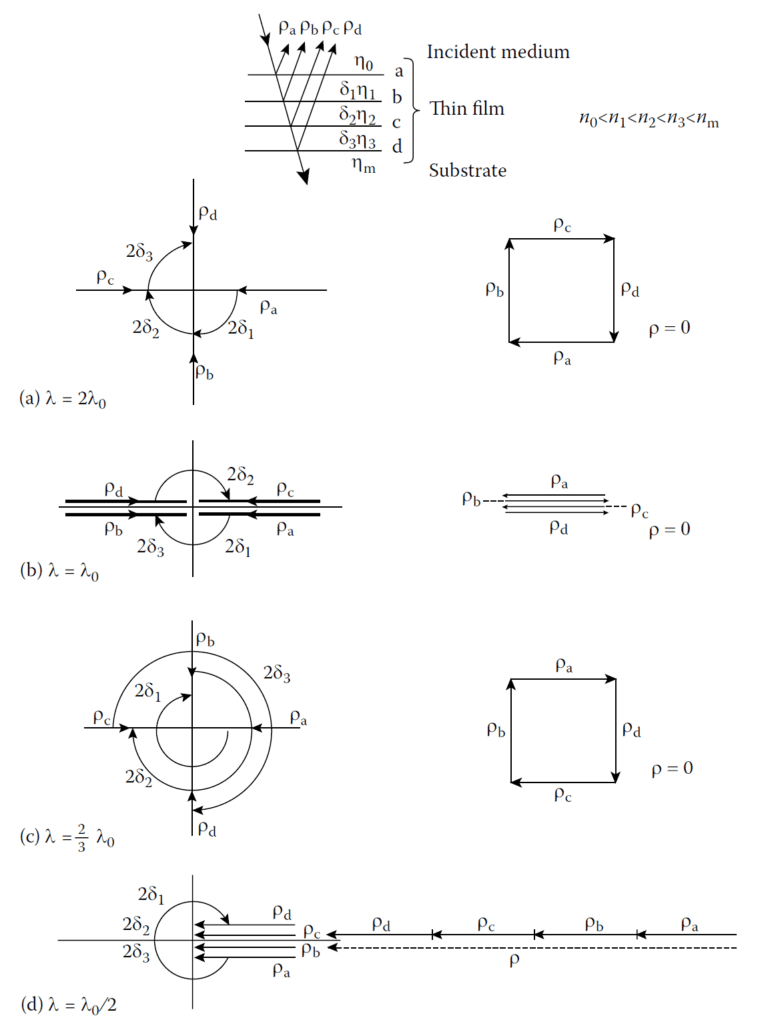
Vector diagram for a quarter-quarter-quarter coating on a high-index substrate ; (a), (b), (c), and
(d) represent wavelengths of 2λ\(_0\), λ\(_0\), (2/3) λ\(_0\), and λ\(_0\)/2 respectively.
Design Conditions
For the vectors to cancel completely, their lengths must satisfy:
\[
\frac{y_1}{y_0} = \frac{y_2}{y_1} = \frac{y_3}{y_2} = \frac{y_m}{y_3}
\]
This leads to the condition:
\[
y_1 = \sqrt[4]{y_0^3 y_m}, \quad y_2 = \sqrt{y_0 y_m}, \quad y_3 = \sqrt[4]{y_0 y_m^3}
\tag{4.12}
\]
For germanium (\( n_m = 4.0 \)) in air (\( n_0 = 1.0 \)), the refractive indices required are:
- \( n_1 = 1.41 \)
- \( n_2 = 2.00 \)
- \( n_3 = 2.83 \)
Practical Design Example
A practical realization of this design uses:
- Layer 1: Silicon \(( n = 3.3 )\)
- Layer 2: Cerium oxide \(( n = 2.2 )\)
- Layer 3: Magnesium fluoride \(( n = 1.35 )\)
Performance of this coating is shown in Figure 4.14, with \( \lambda_0 = 3.5 \, \mu \text{m} \).
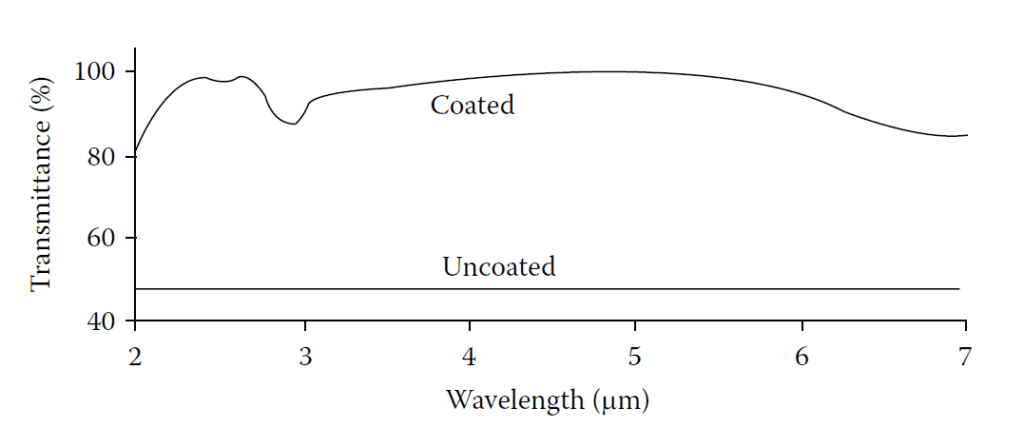
Measured transmittance of a germanium plate with coatings consisting of MgF\(_2\) + CeO\(_2\) + Si
(n\(_1\)d\(_1\)=n\(_2\)d\(_2\)=n\(_3\)d\(_3\)=λ/4 at 3.5 μm).
Extensions to More Layers
The vector method can be extended to coatings with four or more layers:
- Four-layer coatings produce zeros at \( (5/8)\lambda_0, (5/6)\lambda_0, (5/4)\lambda_0, \text{and } (5/2)\lambda_0 \).
- Five-layer coatings yield even broader regions of low reflectance.
These multilayer coatings are analyzed using exact theory, but as the complexity grows, alternative design techniques become more practical.
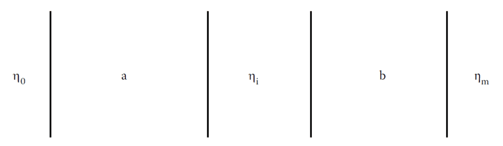
Multilayer antireflection coating consisting of two subsystems a and b separated by a central
layer.
Musset and Thelen Method
Musset and Thelen developed a simplified design method for multilayers based on:
- Breaking down the multilayer into two subsystems (a and b):
- Subsystem \( a \): bounded by \( y_m \) and \( y_i \).
- Subsystem \( b \): bounded by \( y_i \) and \( y_0 \).
- Conditions for maximum transmittance:
- Amplitude condition: \( R_a = R_b \).
- Phase condition: \( \phi_a + \phi_b + 2\delta = m\pi \), where \( \delta \) is the phase thickness of a spacer layer.
System Types
- Type I Systems:
- Admittances are scaled by a constant factor:
\[
y_i = \sqrt{y_0 y_m}, \quad f = \sqrt{\frac{y_0}{y_m}}
\]
- Type II Systems:
- Admittances are scaled reciprocally:
\[
y_i = \frac{y_0 y_m}{y_a}, \quad f = \sqrt{y_0 y_m}
\]
These types ensure that the amplitude condition is satisfied across all wavelengths.
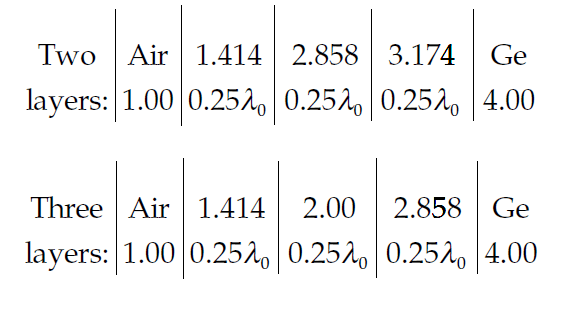
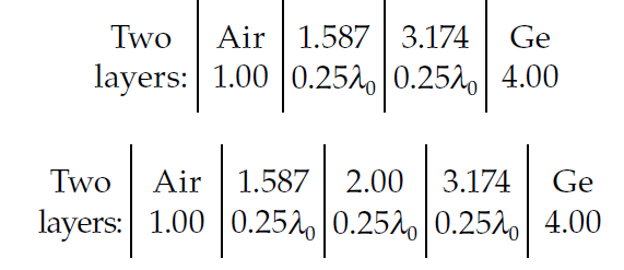
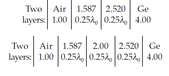
Practical Example: Germanium Coating
For germanium (\( n_0 = 1.00 \), \( n_m = 4.00 \)):
- \( n_i = \sqrt{n_0 n_m} = 2.0 \).
Subsystem designs include:
- Type I:
\[
n_a = 2.826, \quad n_b = 1.414
\] - Type II:
\[
n_a = 2.520, \quad n_b = 1.414
\]
Resulting multilayer designs are shown in Figure 4.16 and Figure 4.17.
Young’s Method
Young proposed another technique using quarter-wave optical thicknesses and drawing parallels with microwave transmission line theory. This method:
- Provides quick designs for given bandwidth and reflectance specifications.
- Does not account for material availability but offers an excellent starting point for real-world coatings.
Multilayer coatings provide substantial flexibility and performance enhancement over single- and two-layer coatings:
- They are suitable for applications requiring broadband performance or low reflectance.
- Techniques like the Musset and Thelen method simplify the design process while ensuring practical implementation.
Theoretical performance of antireflection coatings on germanium designed by the method of
Mussett and Thelen

(a). Theoretical performance of Type I antireflection coatings on germanium designed by the
method of Mussett and Thelen (b). Theoretical performance of Type II antireflection coatings on germanium designed by the
method of Mussett and Thelen