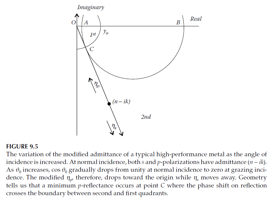
The shift in the modified optical admittance affects the phase shift on reflection from a massive metal. For high-performance metals like silver, the phase shift at normal incidence lies in the second quadrant. As the angle of incidence increases, the movement of the p-polarized admittance toward the origin shifts the phase toward the first quadrant.
Key Features of the Admittance Diagram
1. Isoreflectance Circles:
- Isoreflectance circles intersect the real axis at two points (\(OA \cdot OB = y_0^2\)), with the circle tangent to the metal admittance line at a point \(C\).
- The phase shift at \(C\) is 90°, marking the pseudo-Brewster angle. For silver, with optical constants \(0.075 – i3.41\) in air, this angle is approximately 72°.
2. s- and p-Polarization Reflectance:
- As the angle of incidence increases, s-polarized reflectance rises while p-polarized reflectance drops initially, reaching a shallow minimum before rising to 100% at grazing incidence.
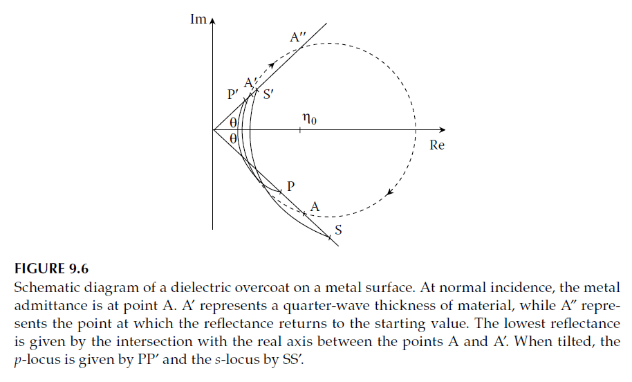
Dielectric Overcoating of Metals
When a metal is overcoated with a dielectric layer, the admittance locus depends on the layer’s admittance (\(\eta_f\)) relative to the metal admittance (\(\eta_m\)):
- For \(\eta_f < \sqrt{\eta_m \eta_m^*}\), the locus loops outside the line from the origin to the starting point.
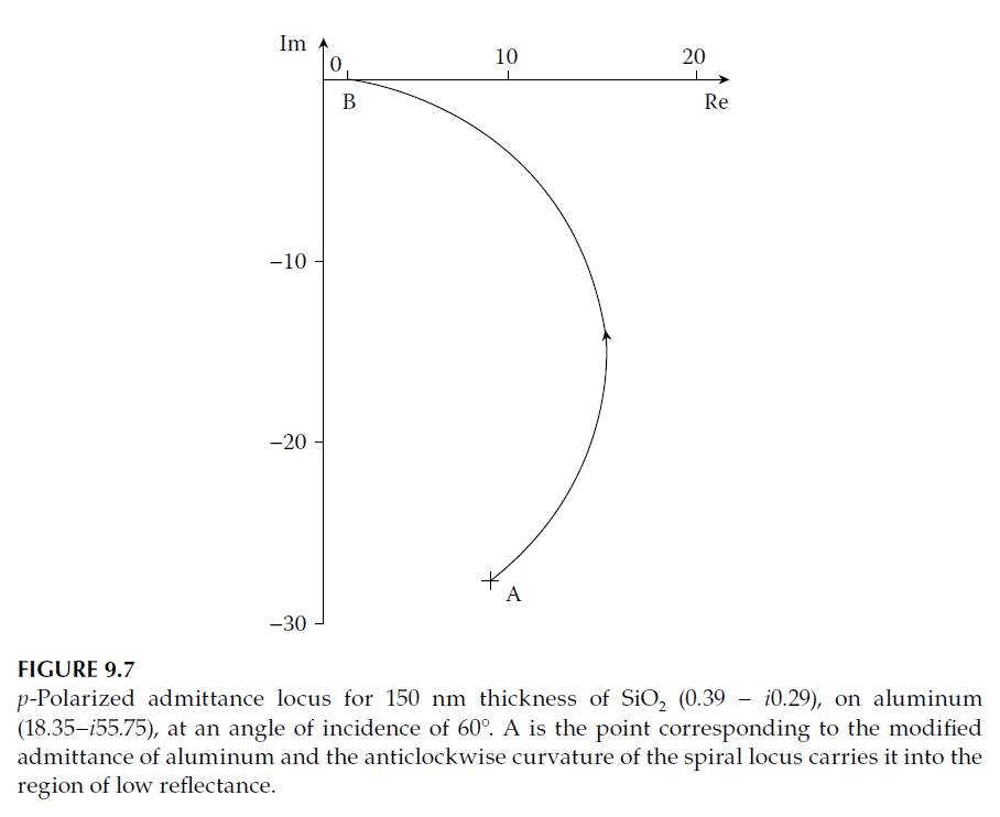
- Reflectance decreases with increasing dielectric thickness until it reaches a minimum, typically at a quarter-wave thickness. For silver, the decrease is slight; for aluminum, it can be significant.
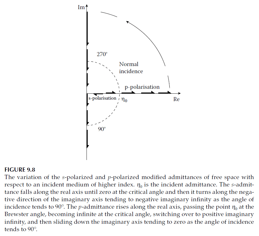
At high angles of incidence:
- The p-admittance of the dielectric layer drops, reducing reflectance.
- The s-admittance increases, raising reflectance. For very high angles, the dielectric layer may enhance reflectance rather than reducing it.
Special Resonances and Surface Plasma Waves
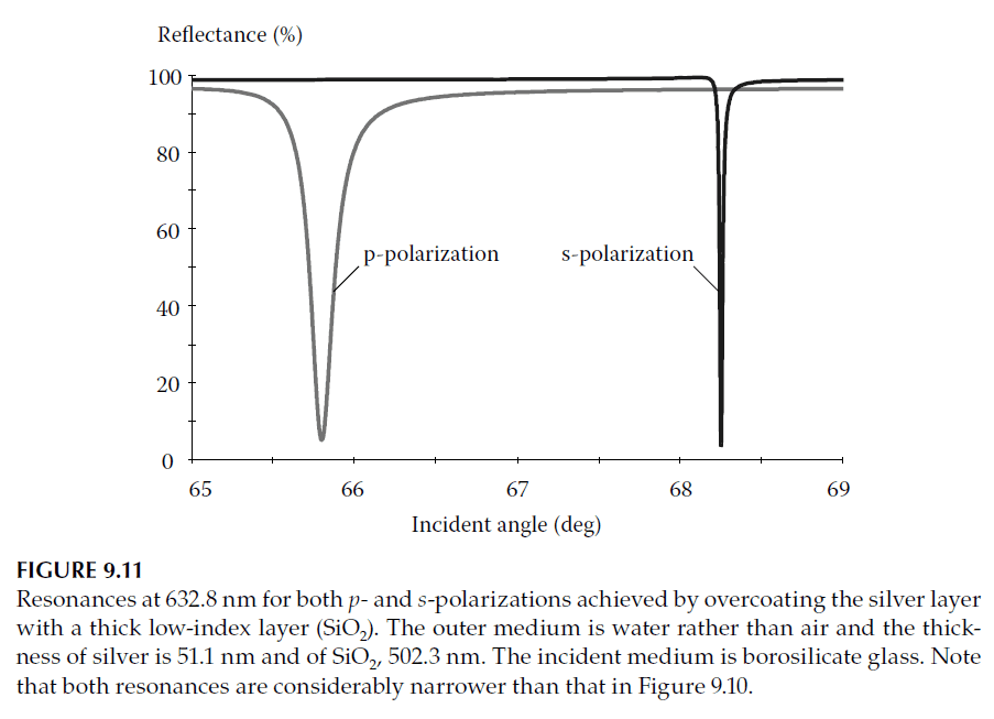
1. Resonance with s-Polarized Light:
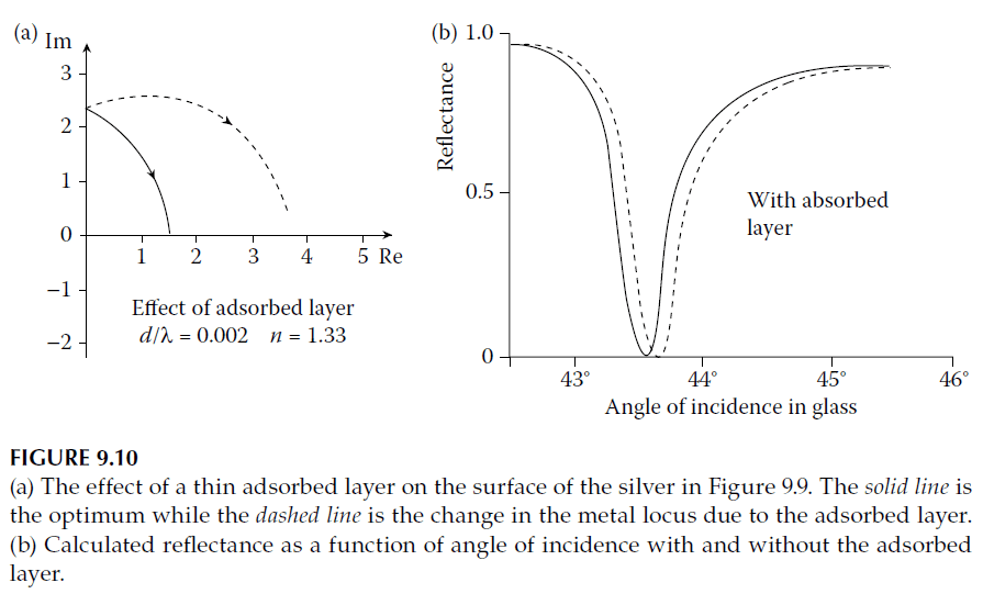
- A thin dielectric layer can shift the metal’s starting admittance, enabling resonances for s-polarized light similar to those for p-polarization.
- These resonances allow high sensitivity to surface layers, enabling the detection of films as thin as a few ångströms.
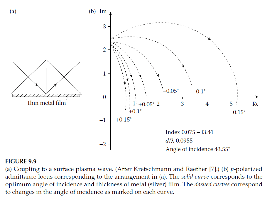
2. Plasmonic Resonances:
- For p-polarized light, coupling to a surface plasma wave occurs at a specific angle and metal thickness. This leads to a sharp resonance with near-zero reflectance, explained by the Kretschmann and Raether configuration.
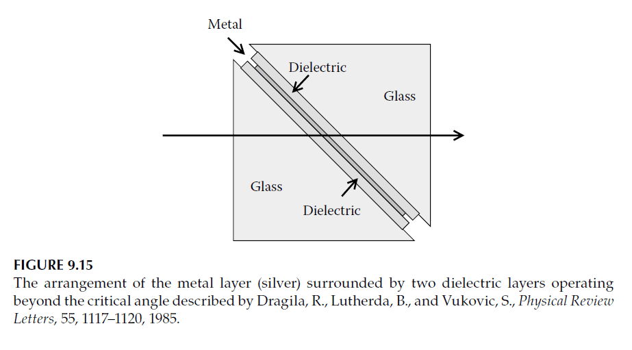
3. Frustrated Total Reflectance (FTR):
- Otto’s configuration excites surface waves through an FTR layer. The dielectric layer beyond the critical angle has a circular locus intersecting the real axis, enabling resonance with a metal substrate.
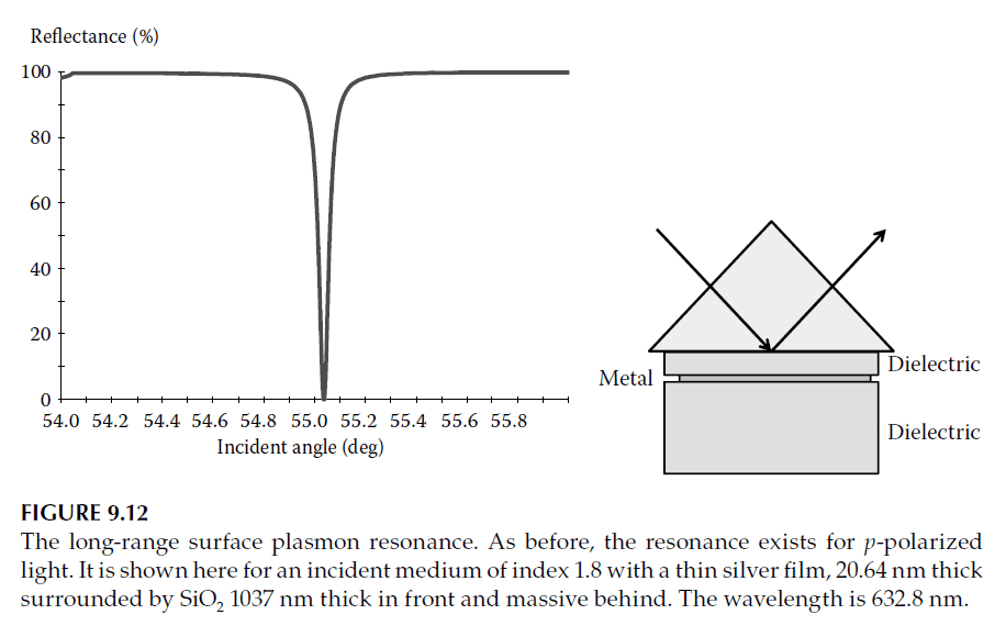
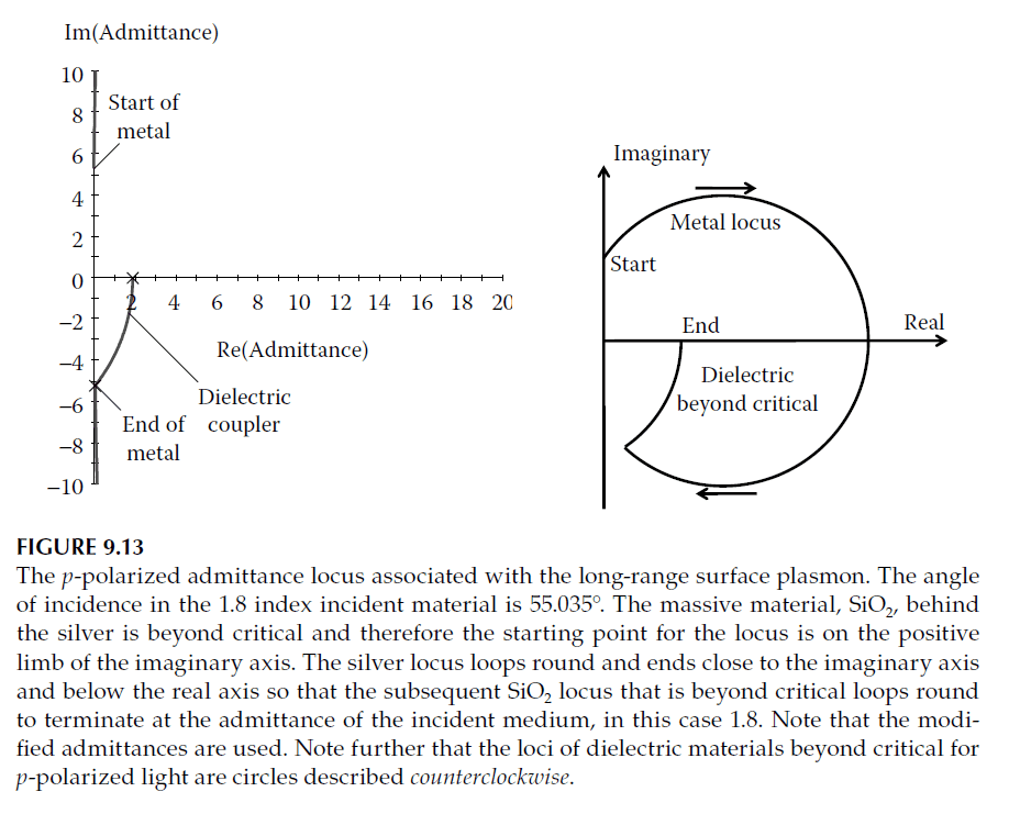
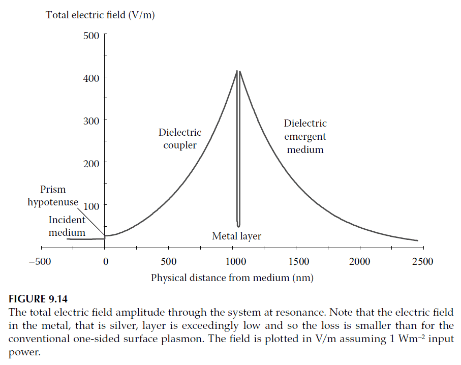
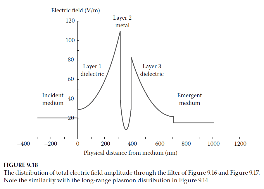
Long-Range Surface Plasmons
A thinner metal layer surrounded by dielectrics beyond the critical angle supports long-range surface plasmons:
- These exhibit extremely narrow resonances and low losses due to minimal electric field penetration into the metal.
- The admittance diagram shows loci looping counterclockwise, terminating at the incident medium’s admittance.
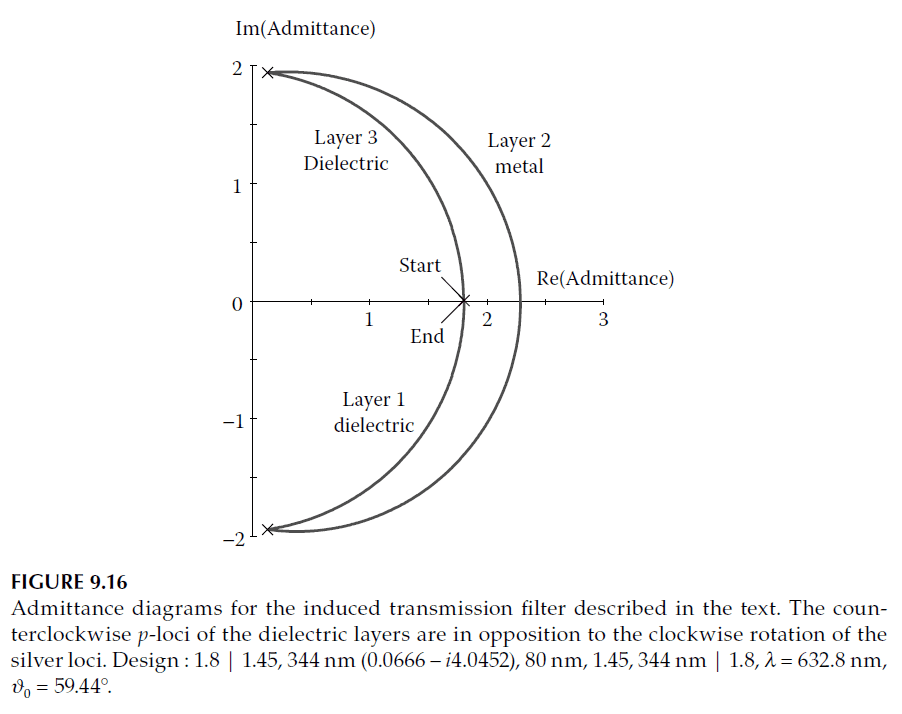
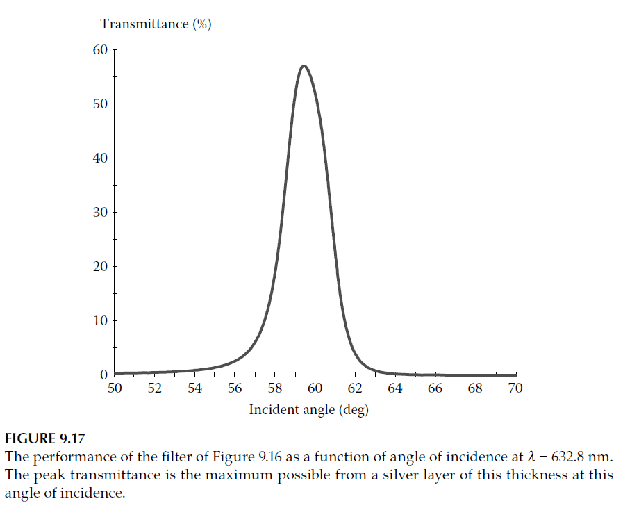
Enhanced Transmission and Metal Transparency
Coupled plasma waves in thin metal layers between dielectric layers can produce unexpected transparency:
- Maximum transmittance is achieved when the admittance at the rear surface matches the optimum value based on layer thickness and optical constants.
- This behavior, explained as an induced transmission filter, aligns with mechanisms used in dielectric–metal–dielectric designs.
Practical Applications
1. Reflection Polarizers:
- Overcoated metals enable the design of reflection polarizers by exploiting the differences in s- and p-polarized reflectance.
2. Biochemical Detection:
- Overcoated systems (e.g., SiO\(_2\) on metals) provide rugged, reusable sensors with high sensitivity to thin biological films.
3. Transmission Filters:
- Regular arrays of holes in metal layers or diffraction gratings enhance transparency, reducing electric field losses in the metal.
Figures and Key Data
Figures (e.g., 9.5–9.18) illustrate:
- Admittance loci for dielectric and metal layers.
- Typical resonances for metal–dielectric systems.
- Enhanced transmission designs and plasmonic effects.