Thin-film coatings are specialized layers applied to surfaces to modify their optical properties, such as how much light passes through (transmittance) or bounces off (reflectance). These coatings are commonly used to enhance or change the performance of optical components and can be categorized into several main types:
- Antireflection (AR): Designed to reduce unwanted reflections that naturally occur at the boundary between different materials, like air and glass.
- High Reflection (HR): Also known as mirror coatings, these increase a surface’s reflectivity, making it more effective at reflecting light.
- Partial Reflection: Used in beamsplitters, which are designed to transmit a specific percentage of light while reflecting the remainder. These coatings are often applied at angles other than perpendicular.
- Polarization: Polarizing coatings separate incoming light into two orthogonal polarized components, typically transmitting one and reflecting the other.
- Filter: These coatings selectively modify optical properties based on the wavelength of light, such as transmitting one wavelength while reflecting another.
Each type serves a unique function, allowing optical devices to perform more efficiently in various applications.
Optical coatings consist of either thin layers of dielectric materials, thicker layers of metals, or a combination of both. The functioning of metal coatings is based on the inherent reflectance and absorption properties of the metallic material itself. In contrast, dielectric thin-film coatings rely on optical interference to achieve their effects.
To illustrate this process, imagine a light ray striking the surface of a material coated with a single-layer thin film. When the light ray reaches the air-coating interface, part of its energy is reflected, while the rest passes through and refracts within the coating. As the refracted light reaches the boundary between the coating and the underlying substrate, some of it is reflected back and some is transmitted further.
The reflected light waves from both interfaces then overlap, and because they are light waves, the resulting reflected light’s amplitude is determined by the complex sum of the amplitudes of these overlapping waves. This interference between the light waves is what gives dielectric thin-film coatings their unique optical properties.

Antireflection coatings are designed to eliminate reflections by making the reflected light waves cancel each other out through destructive interference. This occurs when two reflected light rays have the same amplitude but are precisely half a wavelength (180°) out of phase, resulting in no reflection.
To achieve this phase difference, the second reflected ray must travel an optical path that is exactly half the wavelength of the incoming light before merging with the first ray. When the light is incident at a normal angle (0°), the coating’s optical thickness needs to be one-quarter of the wavelength. Additionally, for the reflected rays to have identical amplitudes, the refractive index of the coating should be the square root of the refractive index of the underlying substrate.
However, these exact conditions can only be met at a specific wavelength and angle of incidence. In many cases, suitable coating materials with the required refractive index for a given substrate may not be available. As a result, while single-layer antireflection coatings are commonly used, more advanced applications often employ multilayer coatings. These complex designs can achieve higher performance, accommodate a broader range of wavelengths and incident angles, and make use of more practical coating materials.
Practical Considerations and Trade-offs in Coating
By applying the fundamental principle of interference, multilayer dielectric coatings can be engineered to reduce or increase reflection at specific wavelengths, or to selectively reflect or transmit certain polarizations. In practical applications, these coatings may consist of dozens or even hundreds of layers, utilizing a variety of available materials to achieve the desired optical effects.
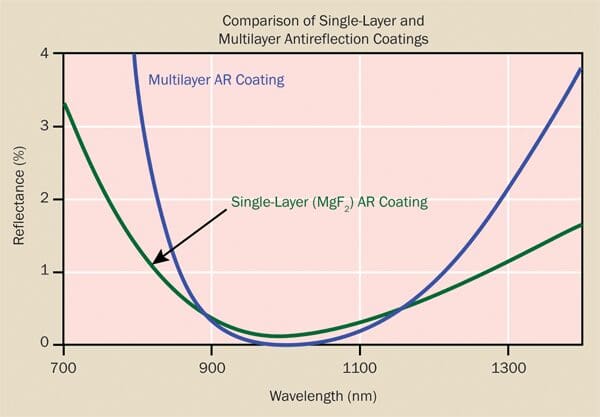
However, the selection of materials available for coating design is limited, meaning practical coatings must be made using a specific range of refractive indices. Additionally, achieving perfect control over the deposition of thickness and refractive index is not feasible. Therefore, it is essential for coating buyers to understand the realistic performance specifications that can be achieved, as well as the factors that can increase costs or lead to other issues, such as reduced mechanical durability or lower laser damage resistance. Below, we review the most common considerations for each of the previously mentioned coating types.
Antireflection Coatings
The performance of an antireflection (AR) coating is usually defined by either the maximum allowable reflectance at a specific wavelength or the average allowable reflectance over a designated wavelength range. When AR coatings are designed for a single wavelength or a specific angle of incidence, achieving high performance is common, with reflectance levels below 0.1% per surface for visible wavelengths on glass substrates.
However, maintaining high performance becomes more challenging as the spectral bandwidth or angular range expands. Therefore, it is important for the buyer to specify whether the required performance applies to the peak value or the average across the entire operational wavelength or angular range. Otherwise, coating costs may increase unnecessarily.
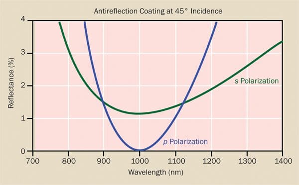
For AR coatings intended to function at nonzero angles of incidence, particularly angles above 30°, the polarization state of the incoming light significantly influences the coating’s design and effectiveness. It is crucial to specify the incident light’s polarization state, which is defined concerning the reflecting surface. The plane formed by the incident and reflected rays is called the “plane of incidence.” Light is considered p-polarized if its electric field vector lies within this plane, and s-polarized if the vector is perpendicular to it. Any other polarization state can be represented as a combination of these s and p components.
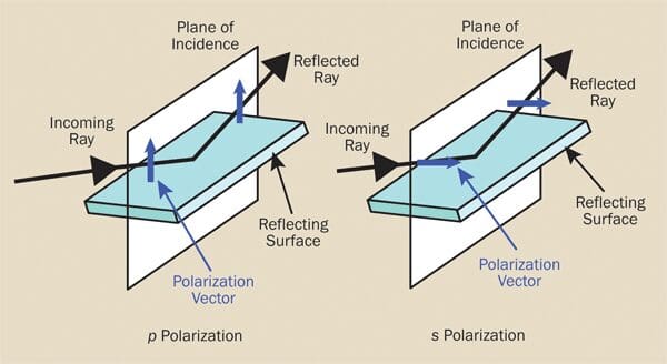
The reflectance of a dielectric interface is always higher for s-polarized light compared to p-polarized light at any nonzero angle of incidence. Thus, if an optical system requires low reflectivity from a tilted component, it is beneficial to design the system so that the component encounters p-polarized light.
It’s also important to distinguish between unpolarized and randomly polarized light. Unpolarized light consists of equal amounts of s and p polarization components, whereas randomly polarized light has an unspecified polarization state, with its direction or ellipticity either unknown or changing over time. This presents a challenge for coating design, as it requires ensuring performance under potentially unfavorable conditions. For example, ambient, incoherent light is typically unpolarized, while laser light emerging from a single-mode optical fiber is often randomly polarized.
Dielectric coatings shift their response toward shorter wavelengths as the angle of incidence increases. For instance, an antireflection coating optimized for minimum reflectance at 532 nm at normal incidence will reflect less at a shorter wavelength when used at a 45° angle. This factor becomes important for coatings on curved surfaces, such as steep aspheric lenses. Here, the angle of incidence can range from 0° at the center to as much as 70° at the edges. As a result, even for a single wavelength, the coating must have a broad enough bandwidth to perform well at the intended wavelength despite this shift. Additionally, applying coatings uniformly on steep surfaces may require special equipment, increasing the complexity and cost.
Antireflection coatings designed for two or more specific wavelengths are common in laser applications. It is generally easier and more cost-effective to achieve high performance at a few discrete wavelengths than to maintain the same level of performance across an entire range. Moreover, specifying high performance for just one wavelength while relaxing requirements for others can help reduce costs further.
Creating multiwavelength antireflection (AR) coatings that function in both the ultraviolet (UV) and visible ranges, or in the visible and infrared (IR), presents challenges due to the limited selection of materials that transmit effectively across these regions. For example, very few coating materials can be used below 250 nm, so working at shorter wavelengths restricts design options and increases costs. Similarly, many materials suitable for the visible spectrum are not effective above approximately 5 µm, making it difficult to produce AR coatings that operate in both deep-UV and visible ranges, or across the near-infrared (NIR) and 10 µm regions.
In many applications, the laser damage threshold is a critical factor. Designing a coating to maximize this threshold may restrict the choice of materials, coating designs, and fabrication methods, which can make it more challenging to meet specific performance requirements, such as achieving a particular reflectance level at a given wavelength or maintaining coating performance over a wide bandwidth.
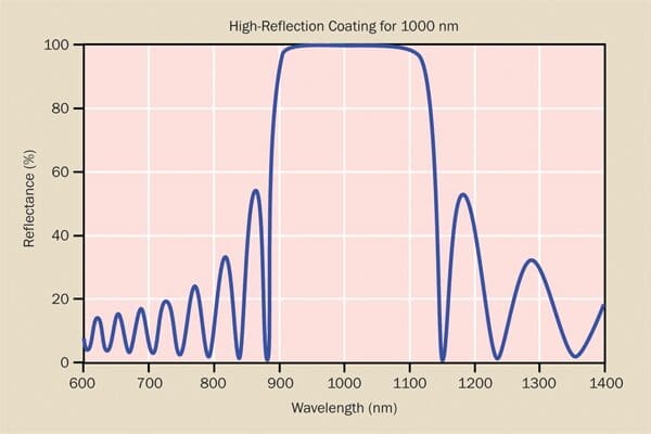
The peak reflectance achieved with metal films falls short compared to dielectric coatings. For instance, gold can achieve 99.5% reflectance in the infrared, but dielectric coatings can consistently deliver 99.99% or higher reflectance, though usually only at a single wavelength. The minor absorption in metal films that limits their reflectance also leads to a significant drawback: susceptibility to damage under high laser fluences.
Metal films also lack the physical durability of all-dielectric coatings, exhibiting lower resistance to abrasion, humidity, thermal cycling, and salt exposure. Silver, in particular, requires a protective overcoat to prevent oxidation, which can significantly reduce its reflectance.
For all-dielectric high reflectors with extremely high reflectivity (≥99.995%), substrate quality becomes critical because surface scatter can limit performance. This means specifying the surface roughness of the underlying substrate, and achieving the required smoothness can increase costs due to the need for specialized polishing techniques.
As with antireflection coatings, there is a trade-off between bandwidth and peak performance in high reflectors, though the impact is less severe. High-reflectivity (HR) coatings typically involve multiple layers, so demanding very broadband performance can increase scatter and absorption, as well as internal stress. This stress may necessitate special techniques to maintain surface figure accuracy.
Beamsplitters and partial reflectors
Nonpolarizing beamsplitters come in two main types: cube and plate. Cube beamsplitters consist of two right-angle prisms joined together at their hypotenuses, where a beamsplitter coating is applied. The input and output faces usually have antireflection (AR) coatings, and they are designed for light entering at normal incidence, with the reflected beam exiting at a 90° angle to the input. Plate beamsplitters, on the other hand, are built on a flat substrate with the beamsplitter coating on the front surface and, typically, an AR coating on the back. These operate at a 45° angle of incidence, with the reflected beam also exiting at a 90° angle from the input. Another type of partial reflector, often used in laser applications, is the laser output coupler, which is typically made on a curved substrate with a long radius and functions at normal incidence.
Cube beamsplitters offer the advantage of being less sensitive to input polarization compared to plate designs. Additionally, in cube beamsplitters, secondary reflections from the input and output faces align with the main beam, whereas, in plate beamsplitters, these reflections are offset.
However, cube beamsplitters have some drawbacks. They are bulkier and heavier than plate beamsplitters, which can be problematic for larger apertures. Additionally, in most cube beamsplitters, the prisms are joined using adhesive or optical contact, which can introduce wavefront errors and reduce performance. The adhesive can also absorb light, leading to scatter and lowering the laser damage threshold.
To address these issues, some manufacturers have developed techniques to prepare the prism surfaces so that a chemical bond forms during assembly. Testing at REO has shown that this approach produces a component with mechanical strength and durability equivalent to a monolithic cube, while avoiding the absorption, scatter, and damage problems associated with adhesive bonding.
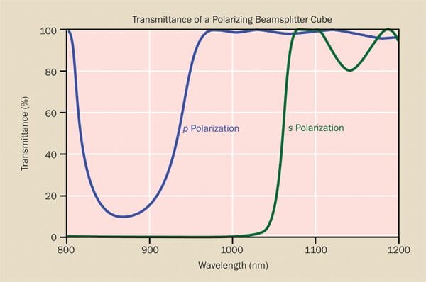
Several factors contribute to the complexity and cost of beamsplitters. One key factor is the angle of incidence: as this angle increases, the difference in reflectivity between s and p polarizations becomes more pronounced, making it increasingly challenging to achieve consistent performance across both polarization states. Therefore, if possible, it is advantageous to work with a single polarization in such cases. However, when using unpolarized light is unavoidable, it is preferable to design the optical system so that beamsplitters operate at lower angles of incidence to reduce the impact of polarization differences.
Careful consideration is needed when specifying tolerances for beamsplitters. There is a significant difference between a beamsplitter that must maintain its specified performance across the entire 45° ±5° incidence range and one that only needs to achieve the required performance at some point within that range. In the first scenario, the beamsplitter must meet performance standards at all angles between 40° and 50°, while in the second scenario, the performance requirements are met somewhere within the 40° to 50° range, with the expectation that the user will fine-tune the component’s tilt to reach the desired performance. The first scenario requires a much more expensive component than the second.
Bandwidth is another critical factor for beamsplitters. Achieving a polarization-insensitive coating that spans more than ±10% of the central wavelength (e.g., 550 nm ±50 nm) presents a significant challenge.
Polarizers
Thin-film polarizers are available in both cube and plate forms. Many plate polarizers are designed for use at or near Brewster’s angle, rather than the typical 45° incidence. Brewster’s angle, where the reflectance of p polarization becomes zero, is approximately 56° for visible wavelengths on glass substrates. Cube polarizers, on the other hand, are typically optimized for around 45° incidence, though higher angles can sometimes offer performance benefits. The trade-offs associated with cube construction, such as bulkiness and potential limitations in laser damage resistance due to adhesive use, are similar to those found in nonpolarizing beamsplitter cubes. Additionally, considerations like specifying the angular range and tilt-tuning apply to cube polarizers as well.
For polarizing beamsplitters, the most critical performance metric is usually the extinction ratio, which measures the ability to separate s and p polarizations. Polarizers are typically designed to transmit p polarization while reflecting s polarization. The transmission extinction ratio is defined as the ratio of p transmission to s transmission (Tp/Ts), while the reflection extinction ratio is defined as the ratio of s reflection to p reflection (Rs/Rp).
When designing systems that incorporate polarizers, it’s important to note that it is generally easier to minimize s-polarized light in the transmitted beam than to completely exclude p-polarized light from the reflected beam. As a result, achieving a transmission extinction ratio of 10,000:1 is feasible, whereas achieving a reflection extinction ratio higher than 100:1 can be challenging and costly. Therefore, tightening the reflection extinction ratio requirements should be carefully considered to avoid unnecessary expense.
Creating thin-film polarizers that perform well across a wide range of wavelengths or at multiple wavelengths is also difficult. It imposes stringent limitations on the choice of substrate and coating materials, as well as the angle of incidence, making it a complex task.
Filters
Filter coatings are designed to have distinct regions of high transmission and high reflection or absorption across different wavelengths. When the wavelengths being blocked are not of concern, bulk absorptive materials, such as colored glass, can be added to enhance out-of-band rejection.
The following figure illustrates three typical transmission curves for long-wave pass thin-film filters. As the slope of the curve becomes steeper, the separation between the highly reflective and transmissive regions decreases. However, an increase in slope also results in more pronounced “ringing” in the transmission band response. The challenge lies in controlling the exact shape and peak positions of these oscillations during the manufacturing process. Consequently, as the gap between the reflective and transmissive wavelengths narrows, achieving high transmission at a precise wavelength becomes more challenging and costly. In applications requiring a very sharp transmission edge, such as Raman spectroscopy, designers may opt for a holographic optical element instead of a dielectric filter to meet these stringent requirements.
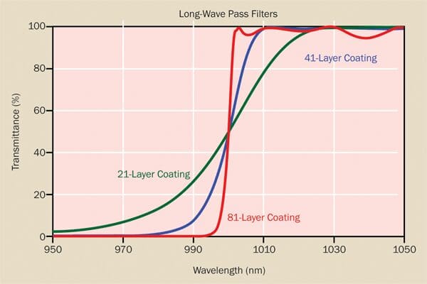
The same manufacturing challenges make it difficult to precisely control the transition wavelength where the coating shifts from reflection to transmission, as well as to accurately set the center wavelength in narrow bandpass filters. By keeping the tolerance for the center wavelength relatively relaxed and allowing the optic to be tilt-tuned during use, component costs can be reduced.
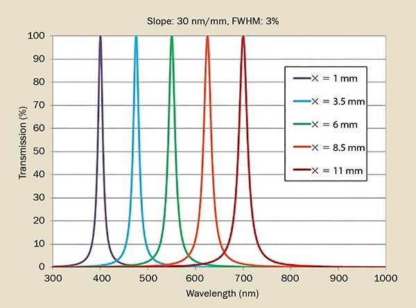
Linear variable filters have spectral properties that change based on their position along the filter. They can be designed as bandpass, long-pass, or short-pass filters. The following figure shows the spectral performance of a linear variable bandpass filter at different points along its length. Key factors for these filters include out-of-band blocking, the accuracy and linearity of the filter’s slope, and the range of slopes that can be produced, which determines the possible filter sizes.
High energy laser (HEL) reflective and transmissive coatings
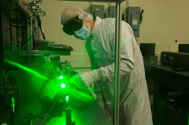
Survivable high-energy laser (HEL) coatings require specific conditions and capabilities to meet essential requirements for coating absorption and defect levels. For HEL applications, optical components must be of higher quality than standard optics, and thin-film coatings need to be made with carefully selected materials and process technologies. The coatings should be applied using ultrapure materials, high-energy deposition methods like ion beam sputtering, and automated process control with proper OH management. Specialized metrology is essential to ensure process consistency and material compliance.
Suppliers should be equipped to perform advanced measurements using cutting-edge techniques, such as photothermal common-path interferometry (CPI) with a sensitivity of less than 0.2 ppm, as well as laser measurements at wavelengths of 1064 nm, 940 nm, 532 nm, and 355 nm. Reports indicate that optimizing high-energy laser components involves automated, nondestructive surface metrology and large-scale defect analysis to enhance laser damage resistance.
Coating fabrication
Thin-film coatings can be created using various technologies, each with its own set of advantages and limitations. However, some manufacturers specialize in just one or two methods, often promoting the benefits of their preferred techniques. This has led to customer confusion and misconceptions regarding the advantages and suitability of different coating processes. In reality, multiple coating methods exist because they each serve a purpose: one technique may be ideal for complex, multispectral laser applications, while another may be better suited for coatings used in humid environments. Although customers don’t need to be experts in thin-film coating methods, understanding the features of the available options can be helpful. Additionally, working with a vendor experienced in a range of techniques can provide a more objective approach when recommending the best solution.
E-beam and thermal evaporation
Evaporative coatings are created within a high-vacuum chamber, where both metallic and dielectric materials can be used. The coating material is heated, either by resistive heating or electron beam bombardment, until it vaporizes. The resulting vapor then travels away from the source and recondenses onto any surfaces that are directly exposed to the source.
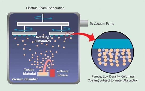
Since no energy is applied during the vapor condensation process, thin films produced by this method tend to be porous, relatively low in density, and have a columnar structure. To mitigate these effects, substrates are typically heated to several hundred degrees Celsius during coating, though this only reduces, rather than eliminates, the porosity.
The porous nature of evaporative films can lead to moisture absorption, causing shifts in coating performance with changes in temperature and humidity. The low density also affects mechanical durability, although these films can still generally meet most MIL-SPEC durability and environmental standards. Additionally, heating the components during processing can limit the choice of substrate materials and may introduce stress from thermal cycling.
Evaporative coating processes are challenging to fully automate and usually require operator supervision. However, the high deposition rates make coating times relatively short, keeping production costs low. This method is especially popular when cost is a key factor and the performance and durability requirements are not too stringent. Another significant advantage of evaporative methods is their compatibility with a wide range of coating materials, including deep-UV fluorides, visible-range oxides, and infrared semiconductors and sulfides.
Ion-assisted deposition (IAD)
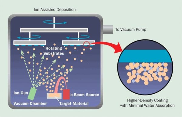
Ion-assisted deposition (IAD) builds on the evaporative coating method by introducing a high-energy ion beam directed at the surface being coated. These ions transfer energy to the deposited material, functioning like a microscopic hammer to achieve higher film density than with traditional evaporation alone. The ion beam can also be used for precleaning or etching the substrate surface, enhancing film adhesion. This combination of a relatively low-temperature deposition process and ion precleaning allows for coating plastic substrates, such as polycarbonate lenses or visors, as well as enabling deposition on the ends of jacketed fibers and over photoresist masks.
IAD coatings typically exhibit greater mechanical durability, better environmental stability, and lower light scatter compared to purely evaporative films. The process offers significant flexibility, as the amount of energetic assistance can be adjusted from zero to a maximum level for each layer. Although some commonly used materials for infrared and deep-UV applications may not be compatible with IAD, the method can still be applied to the outermost layer to enhance the overall durability of the coating. Additionally, ion energy can be used to modify the intrinsic stress of a film during deposition, potentially shifting it from tensile to compressive. This adjustment helps maintain the substrate’s surface shape, especially when applying thick infrared coatings.
Ion-beam sputtering (IBS)
In ion beam sputtering (IBS), a high-energy ion beam is aimed at a target, usually made of a metal or oxide. The ions transfer their momentum to the target material, causing atoms or molecules to be ejected from the surface. These energetic atoms then travel and deposit onto the components being coated. During this process, oxygen is often introduced into the coating chamber as a reactant. It either forms oxides when metal targets are used or reoxidizes any free atoms that have been dissociated during the sputtering process with oxide targets.
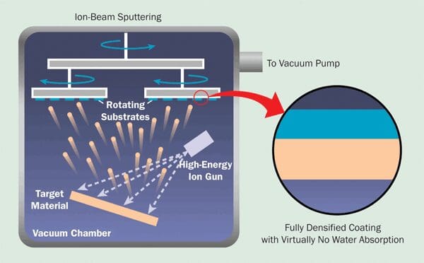
Ion beam sputtering (IBS) creates uniform, highly dense, and completely amorphous films with no porosity, offering excellent adhesion. The coated layers also demonstrate outstanding adhesion properties, extremely low absorption, and minimal surface roughness, even reaching sub-angstrom levels. For instance, in the visible and infrared ranges, IBS films can achieve a combined scatter and absorption of less than 1 ppm.
Although the deposition rates are slower compared to other coating methods, IBS excels in control and reproducibility, allowing for precise performance targeting that surpasses evaporative techniques. This makes IBS particularly suitable for producing steep edge filters, very broadband mirrors, and multiwavelength mirrors and antireflection (AR) coatings. Additionally, the IBS process is highly automatable, eliminating the need for operator supervision.
The main limitation of IBS is its compatibility with only a narrow range of materials, typically metal oxides. Most of these materials are not transmissive below 250 nm or above roughly 5 µm. However, with carefully chosen materials and optimized process parameters, IBS can achieve high-performance coatings at wavelengths as short as 190 nm.
Magnetron sputtering
In magnetron sputtering, the target material is maintained at a negative voltage and placed within a magnetic field. This setup generates a plasma above the target, and the negative potential accelerates ions toward the material. When these ions collide with the target, they cause material to be sputtered off. Additionally, secondary electrons emitted from the target are trapped by the magnetic field, which helps sustain the plasma by facilitating ionizing collisions.
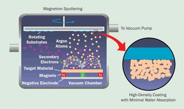
There are several variations in the implementation of magnetron sputtering, tailored to the desired target materials and deposition parameters. For instance, pure metal targets can be powered by a DC supply, while semiconductors and dielectrics typically require either radio frequency or pulsed DC. Deposition can occur with or without a reactive gas, depending on whether oxide formation is intended.
Magnetron sputtering generally strikes a balance between evaporative techniques and ion beam sputtering (IBS) in terms of cost, quality, and performance. It offers higher deposition rates than IBS and can use nearly the same range of materials. While the energy of the deposited atoms in magnetron sputtering is not as high as that achieved with IBS, it is still greater than that of evaporative methods, resulting in excellent coating durability and stability. However, one limitation of magnetron sputtering is that the source typically needs to be positioned much closer to the substrate compared to other coating processes. This proximity can compromise coating uniformity—especially on parts with steep radii of curvature—and surface quality when compared to IBS. Additionally, it is more challenging to control deposition parameters as precisely with magnetron sputtering as it is with IBS, placing this technique in the middle range of achievable precision. Overall, magnetron sputtering is a suitable option when film durability and stability, along with cost considerations, are important, but the highest performance in terms of precision, scatter, and absorption is not critical.
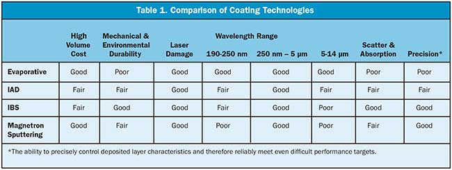
Table 1 provides a quick comparative overview of various coating technologies. However, since there are many different implementations of each technique, this information should serve as a starting point for discussions with your coating supplier.
Conclusion
In conclusion, nearly all optical systems today incorporate thin films in some capacity, and in many instances, the performance of these coatings is crucial for system functionality. Practical coatings typically involve trade-offs among various performance parameters and costs, where even minor changes in specifications can lead to significant impacts.
Additionally, different deposition technologies present varying capabilities and cost structures. Given these factors, it is often beneficial to collaborate with an optics and coatings vendor that provides a comprehensive range of design and fabrication services, enabling them to identify the best solution to meet all critical requirements for a specific application.
