Multilayer Dielectric Coatings
In previous tutorials, it was mentioned that a high reflectance can be obtained from a stack of quarter-wave dielectric layers with alternating high and low refractive indices. This is because beams reflected from all the interfaces in the assembly are of equal phase when they reach the front surface, where they combine constructively.
An expression is provided in Section 3.1 for the optical admittance of a series of quarter-waves. If \( n_H \) and \( n_L \) are the indices of the high- and low-index layers, and if the stack is arranged so that the high-index layers are outermost on both sides, then:
\[
Y = \frac{n_H^{2p} + n_L^{2p}}{n_{sub}},
\]
where \( n_{sub} \) is the refractive index of the substrate, and \( 2p + 1 \) is the number of layers in the stack.
The reflectance in air or free space is then:
\[
R = \left( \frac{n_H^{2p} – n_L^{2p} + n_{sub}^2}{n_H^{2p} + n_L^{2p} + n_{sub}^2} \right)^2. \tag{6.11}
\]
The greater the number of layers, the higher the reflectance. Maximum reflectance for a given odd number of layers is always obtained with the high-index layers outermost.
If:
\[
n_H^{2p} + n_L^{2p} > n_{sub}^2,
\]
then:
\[
R \approx 1 – \frac{4n_L^{2p} n_{sub}^2}{n_H^{2p}},
\]
and:
\[
T \approx \frac{4n_L^{2p} n_{sub}^2}{n_H^{2p}}. \tag{6.12}
\]
This shows that when reflectance is high, the addition of two extra layers reduces transmittance by a factor of \( \left( \frac{n_L}{n_H} \right)^2 \).
Absorption and Transparency
Provided the materials are transparent, the absorption in a multilayer stack can be negligible. For the visible region of the spectrum, absorptance can be less than 0.01%.
Phase Shift and Bandwidth
Dielectric multilayers, however, suffer from two issues:
- Variable phase shift: This occurs with reflection and varies depending on the wavelength.
- Limited bandwidth: High reflectance is achieved over a restricted range of wavelengths.
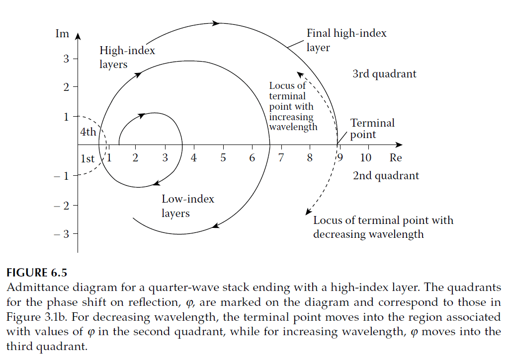
Using the admittance diagram, we can see how phase shift varies:
- For a stack with high-index layers on the outside, the phase shift at the design wavelength is \( \pi \). As the wavelength increases, the phase shift also increases, moving into the third quadrant. For shorter wavelengths, the phase shift decreases, moving into the second quadrant (Figure 6.5).
- For a stack ending with a low-index layer, the phase shift at the reference wavelength is zero, moving into the first or fourth quadrant as the wavelength changes.
Effect of Phase Change on Transmission Peaks
Allowing for phase changes \( \phi_a \) and \( \phi_b \), the transmission peaks shift from \( \delta = m\pi \) to:
\[
\delta = q\pi – \phi_a + \phi_b,
\]
where \( q = 0, \pm1, \pm2, \dots \). The shifts are small in high-order systems, and phase effects can be eliminated by using spacers of different thicknesses, as described by Stanley and Andrew.
High-Reflectance Zones
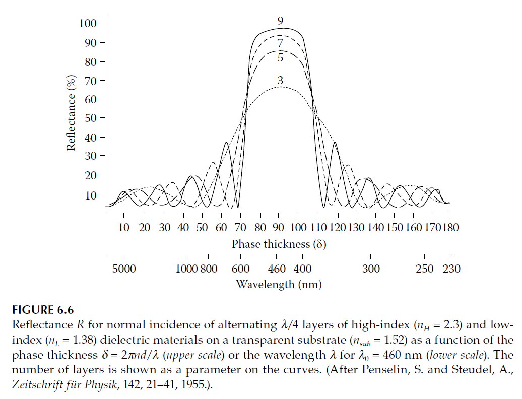
The behavior of a typical quarter-wave stack is shown in Figure 6.6. The high-reflectance zone is limited in extent, with reflectance dropping sharply outside this range. Adding layers increases reflectance within the zone but does not widen it.
The width of the high-reflectance zone is:
\[
\Delta g = \frac{2}{\pi} \arcsin \left( \frac{n_H^2 – n_L^2}{n_H^2 + n_L^2} \right),
\]
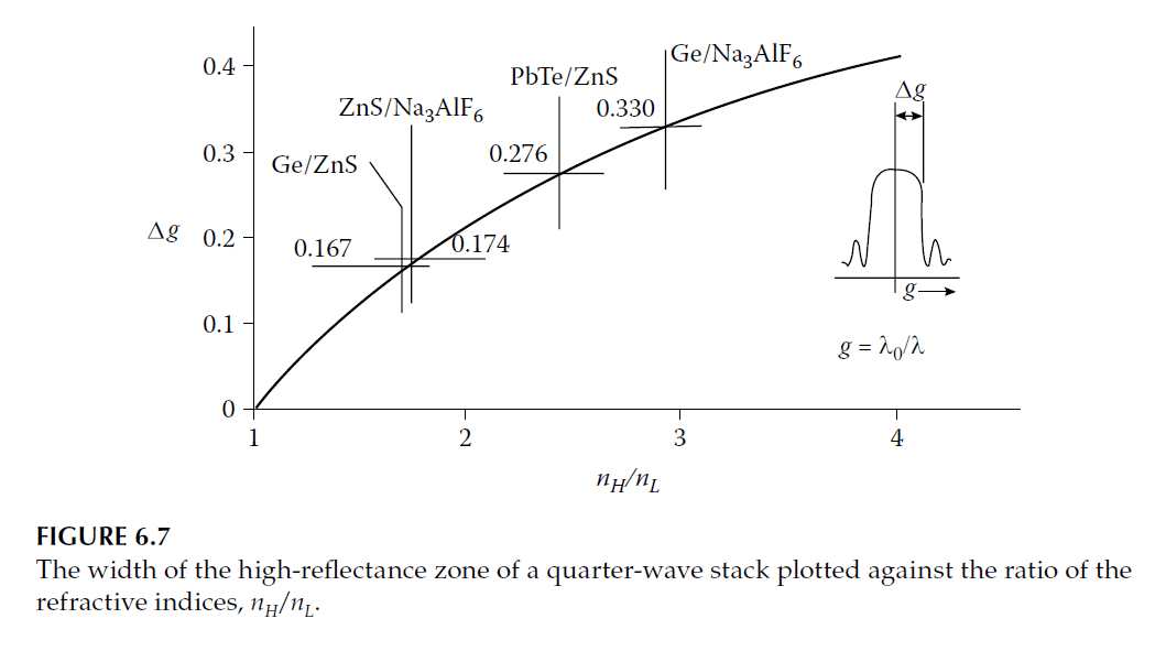
where \( \Delta g \) depends on the refractive indices of the materials. Figure 6.7 plots \( \Delta g \) against the ratio of refractive indices.
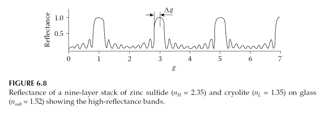
High-reflectance zones exist at odd multiples of the fundamental wavelength \(( \lambda_0/3, \lambda_0/5, \dots )\). At even multiples, the layers act as absentee layers, reducing reflectance to that of the uncoated substrate.
Materials and Practical Considerations
Material choice depends on the wavelength range and application:
- Visible spectrum: Zinc sulfide and cryolite are traditional materials, but oxides like silicon dioxide, titanium dioxide, and tantalum pentoxide are more durable. Figure 6.8 shows reflectance curves for higher-order zones.
- UV region: Antimony trioxide and cryolite can replace zinc sulfide for shorter wavelengths.
- Infrared region: Germanium and lead telluride are suitable for wavelengths beyond 1.8 μm.
Preparation techniques greatly influence coating performance. Oxides require electron beam sources due to high evaporation temperatures, while zinc sulfide and cryolite can be evaporated from simple thermal sources. For demanding applications like laser mirrors, extreme care is needed, as detailed in Perry and Heitmann.
All-Dielectric Multilayers with Extended High-Reflectance Zones
The limited range of high reflectance achievable with a quarter-wave stack presents challenges for certain applications. Efforts to extend this range have focused on modifying the layer design, such as staggering the thicknesses of successive layers to create a regular progression. This ensures that across a broad wavelength range, enough layers in the stack maintain optical thicknesses near a quarter-wave to achieve high reflectance.
Harmonic and Geometric Progressions in Layer Design
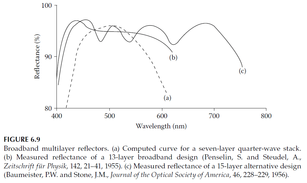
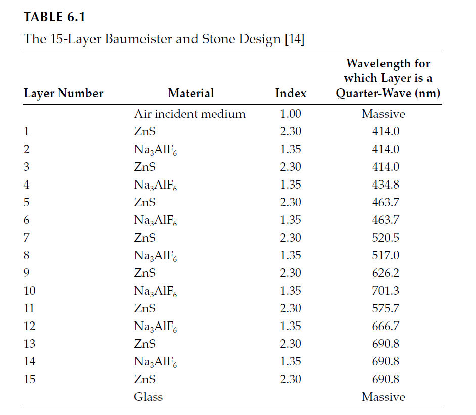
Penselin and Steudel were among the first to explore this method, using harmonic progressions for layer thicknesses. Their results, for a 13-layer stack, are shown as curve B in Figure 6.9. Baumeister and Stone later developed computer-optimized reflectors, achieving significant improvements. Their best 15-layer design is represented by curve C in Figure 6.9.
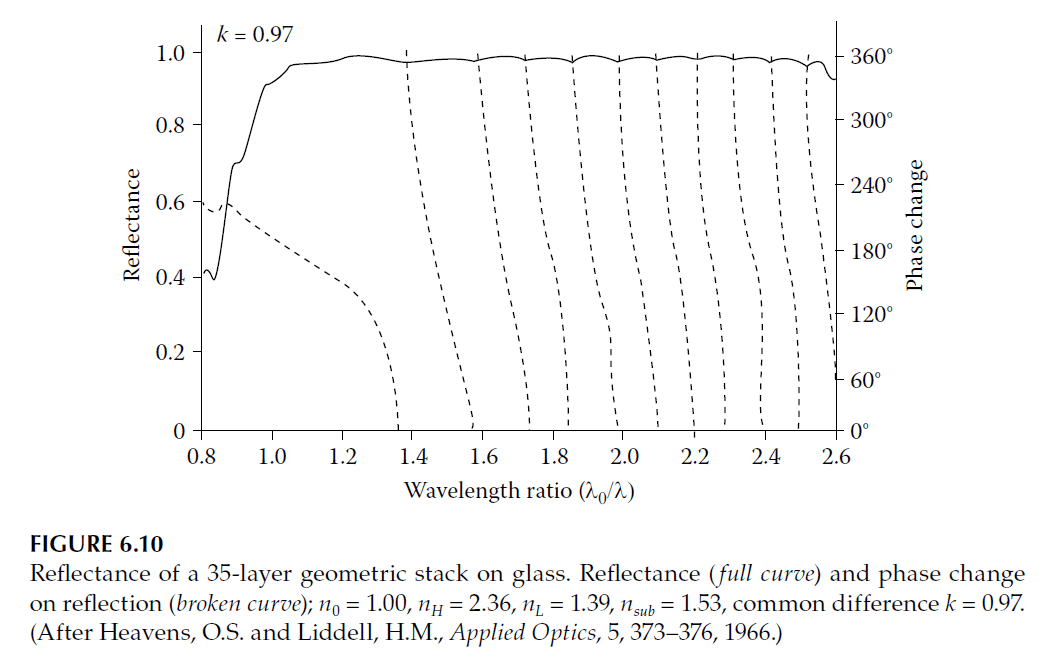
Heavens and Liddell used both arithmetic and geometric progressions to calculate reflection curves for multilayers. Their computations assumed \( n_H = 2.36 \) (zinc sulfide), \( n_L = 1.39 \) (magnesium fluoride), and a glass substrate \(( n = 1.53 )\). Geometric progression offered slightly broader reflection zones compared to arithmetic progression. A 35-layer geometric design is illustrated in Figure 6.10.
Computer-Optimized Multilayers
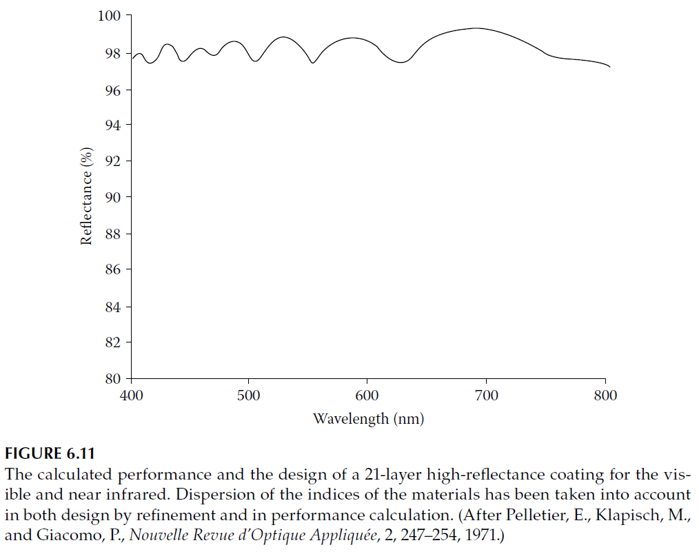
Baumeister and Stone pioneered computer-aided optimization for multilayers. They began with a preliminary 15-layer design using zinc sulfide \(( n = 2.3 )\) and cryolite \(( n = 1.35 )\) on glass, aiming for reflectance around 95%. The final design, refined by an IBM card-programmed calculator, is shown as curve C in Figure 6.9, with design details in Table 6.1. Later advancements, such as those by Pelletier et al., incorporated dispersion effects in the calculations, as shown in Figure 6.11.
Stacked Quarter-Wave Layers for Broad Reflectance
A simple method for broadening reflectance involves stacking quarter-wave designs for two different wavelengths. However, if each stack has an odd number of layers and outermost layers of the same index, a peak of transmission occurs in the middle of the high-reflectance zone. This behavior is analogous to a Fabry–Perot interferometer, where unity transmittance occurs for:
\[
\phi_a + \phi_b – 2\delta = 2q\pi, \quad q = 0, \pm1, \pm2, \dots
\]
This situation is sketched in Figure 6.12, where the two stacks act like a Fabry–Perot cavity with a spacer layer of air. At the mean of the two center wavelengths, \( \phi_a + \phi_b = 2\pi \), and the transmittance reaches unity if \( \delta = 0 \).
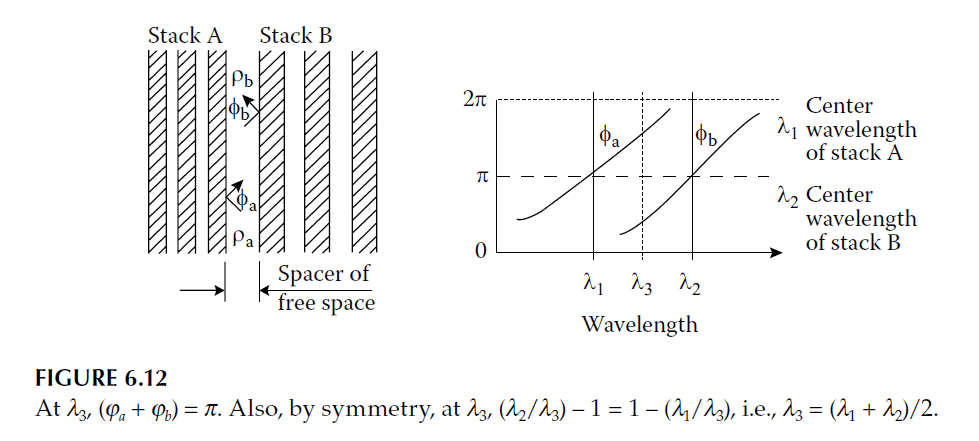
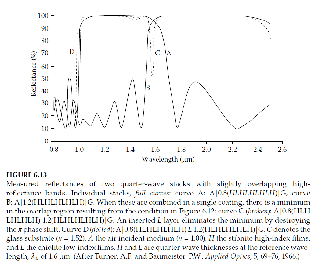
Figure 6.13 illustrates this phenomenon. Curves A and B represent reflectance for two individual quarter-wave stacks, while curve C shows the combined reflectance with a dip caused by the transmission peak.
Suppressing Transmission Peaks
To eliminate the transmission peak, Turner and Baumeister introduced a low-index layer, one quarter-wave thick at the mean wavelength, between the two stacks. This adjustment shifted \( \delta \) to \( \pi/2 \), minimizing transmission and maximizing reflectance. Curve D in Figure 6.13 demonstrates the resulting flat-topped reflectance.
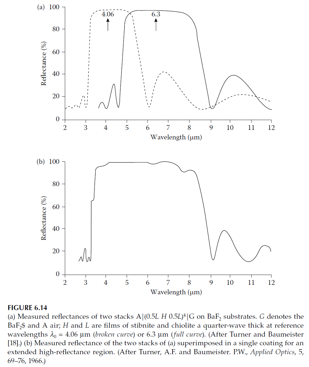
Turner and Baumeister also designed broadband reflectors by considering the multilayer as a single layer with a real optical admittance, except in high-reflectance zones where the admittance becomes imaginary. Figure 6.14a shows reflectance measurements for two stacks on a barium fluoride substrate, illustrating designs where high-reflectance zones either touch or overlap. Overlapping zones suppress minima due to the central layer’s quarter-wavelength thickness.
Coating Uniformity Requirements
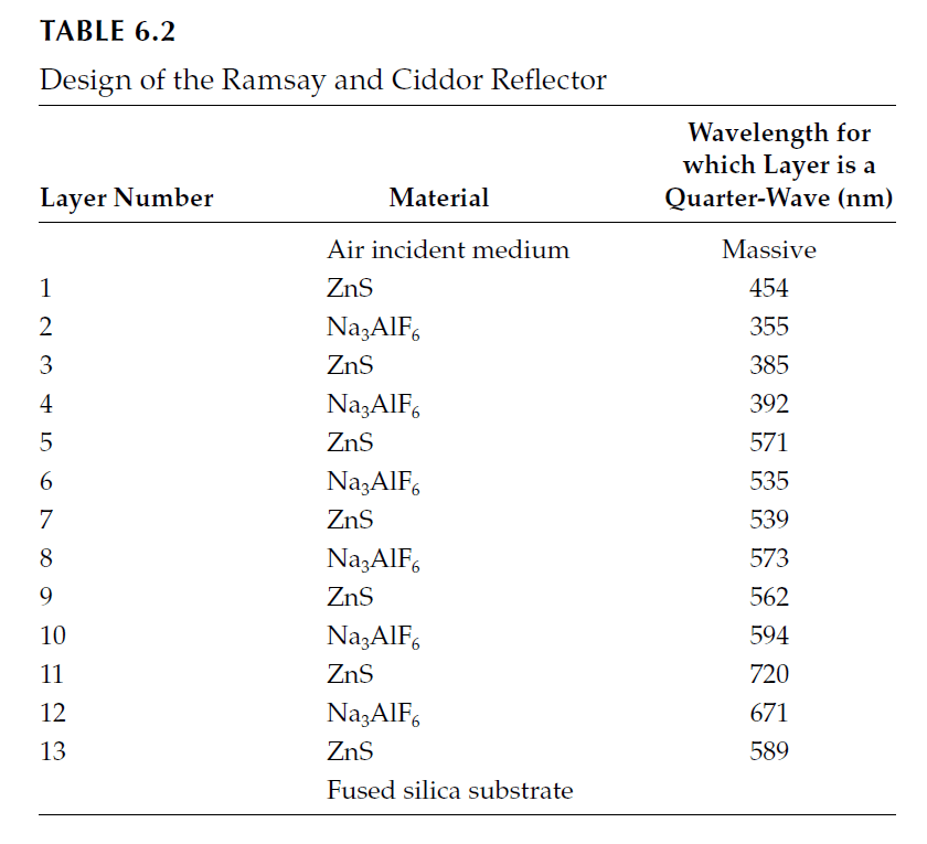
Broadband reflectors, like those previously discussed, exhibit rapid variations in the phase shift on reflection with changes in wavelength, much more so than simple quarter-wave stacks. This can create challenges for determining wavelength in a Fabry–Perot interferometer. Although the dual-spacer method proposed by Stanley and Andrew eliminates the effects of rapid phase shifts, another issue related to coating uniformity was dramatically illustrated in a report by Ramsay and Ciddor.
The Impact of Non-Uniform Coatings
Ramsay and Ciddor investigated a 13-layer coating with a design similar to Baumeister and Stone’s, as listed in Table 6.2. The coating, applied with a layer uniformity of 1–2 nm across 75 mm diameter plates, showed varying apparent curvatures:
- λ/60 concave at 546 nm,
- uniform at 588 nm,
- λ/10 convex at 644 nm.
This apparent curvature is caused not by the physical shape of the plates (confirmed to be λ/60 concave using silver layers) but by variations in coating thickness combined with the phase change on reflection.
Theoretical Explanation
Giacomo published a theory in 1958 that explained this phenomenon and provided estimates of the required uniformity. He showed that the apparent variation in spacer thickness (in units of phase) is proportional to the uniformity error in coating thickness, multiplied by:
\[
\nu \frac{\partial \phi}{\partial \nu} + 4 \pi \nu e,
\]
where:
- \( e \) = total physical thickness of the coating,
- \( \nu = 1/\lambda \) = wavenumber,
- \( \phi \) = phase change on reflection.
The maximum allowable spacer thickness variation \( \Delta \rho_m \) due to non-uniformity requires coating uniformity better than:
\[
\Delta e = \frac{\Delta \rho_m}{e \left( \frac{\partial \phi}{\partial \nu} + 4 \pi \nu \right)}.
\]
The terms \( \frac{\partial \phi}{\partial \nu} \) (generally negative) and \( 4\pi e \) can cancel each other out partially, making some coatings more sensitive to uniformity errors than others.
Observations by Ramsay and Ciddor
Ramsay and Ciddor extended Giacomo’s analysis, showing that:
- The magnitudes of \( \frac{\partial \phi}{\partial \nu} \) and \( 4 \pi e \) vary across the high-reflectance zone, sometimes leading to apparent curvatures that shift between concave and convex.
- This effect means interferometers must be tested for flatness across the entire working range, not just at one wavelength.
Comparison of Quarter-Wave and Broadband Coatings
For quarter-wave coatings, the term \( \frac{\partial \phi}{\partial \nu} \) is much smaller than \( 4 \pi e \). For example:
- A seven-layer zinc sulfide and cryolite coating in the visible spectrum has \( \frac{\partial \phi}{\partial \nu} \approx -1.5 \, \mu\text{m} \) compared to \( 4 \pi e \approx +21.5 \, \mu\text{m} \).
In contrast, broadband multilayers have much larger \( \frac{\partial \phi}{\partial \nu} \). Giacomo reports cases where \( \frac{\partial \phi}{\partial \nu} \) reached \( -125 \, \mu\text{m} \), overwhelming the \( 4 \pi e \) term. Heavens and Liddell note variations in \( \frac{\partial \phi}{\partial \nu} \) from \( 10 \, \mu\text{m} \) to \( 26 \, \mu\text{m} \) for staggered multilayers, making apparent curvature changes inevitable.
Designing Coatings for Reduced Sensitivity
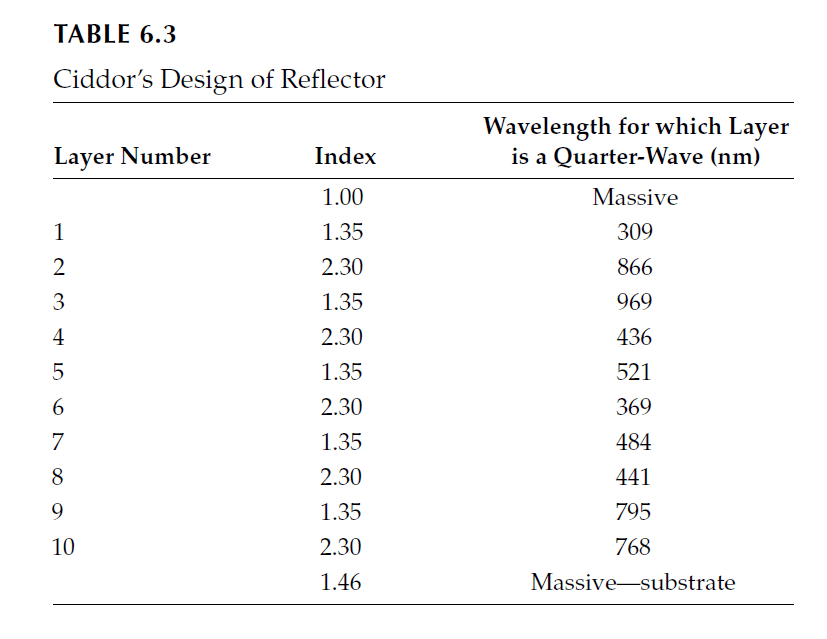
It is possible to design coatings where \( \frac{\partial \phi}{\partial \nu} \) and \( 4 \pi e \) nearly cancel across the working range. Ramsay and Ciddor and later Ciddor developed such designs, achieving significantly reduced sensitivity to thickness variations.
One notable design achieved:
- ~75% reflectance across the visible spectrum,
- ~3x reduced sensitivity to thickness errors compared to designs with no phase change effects.
This design used zinc sulfide \(( n = 2.30 )\) and cryolite \(( n = 1.35 )\) on a fused silica substrate \(( n = 1.46 )\), with layer thicknesses listed in Table 6.3. The reflectance varied within ±2% across 650–400 nm, making the coated interferometer plate appear much flatter than its physical non-uniformity would suggest.
Losses
The reflectance of a quarter-wave stack, assuming lossless materials, depends solely on the number of layers. With high reflectance, adding additional layer pairs reduces transmittance by a factor of \( (n_L/n_H)^2 \). In practice, however, losses—whether from scattering or absorption—limit the achievable reflectance.
Types of Losses
- Scattering Losses:
- Arise from defects such as dust, surface roughness, or imperfections in the layers.
- Mitigated by meticulous preparation, attention to detail, and maintaining clean environments during deposition.
- Absorption Losses:
- Inherent to the material or caused by impurities, structural issues, or composition.
- Proportional to the extinction coefficient \( k \) of the material.
- More impactful on reflectance than on transmittance in multilayer systems.
Absorption Loss in Weakly Absorbing Layers
For a stack of weakly absorbing layers with small \( k \), the absorptance \( A \) can be calculated. Using the concept of potential transmittance \( \psi \):
\[
\psi = \frac{T}{1 – R}
\]
where \( T \) is transmittance and \( R \) is reflectance. For a multilayer assembly:
\[
1 – \psi = A_f,
\]
where \( A_f \) is the absorptance of each layer. For weak absorption, \( \psi \approx 1 \), and the total absorptance \( A \) for the assembly becomes:
\[
A = (1 – R) \sum A_f,
\]
where \( A_f \) for a single quarter-wave layer is:
\[
A_f = \beta \left( \frac{n}{y_e} + \frac{y_e}{n} \right),
\]
with \( \beta = 2 \pi k d / \lambda \), and \( y_e \) being the admittance of the medium.
Absorptance of the Stack
The absorptance for a stack terminating with a high-index layer is given by:
\[
A = \frac{2 \pi n_0}{n_H + n_L} \left( \frac{k_H}{n_H – n_L} + \frac{k_L}{n_H + n_L} \right),
\]
and for a stack terminating with a low-index layer:
\[
A = \frac{2 \pi n_0}{n_H + n_L} \left( \frac{k_L}{n_H – n_L} + \frac{k_H}{n_H + n_L} \right).
\]
Example Calculations
For a multilayer with \( k_H = k_L = 0.0001 \), \( n_H = 2.35 \), \( n_L = 1.35 \), and \( n_0 = 1.00 \):
- High-index layer outermost: \( A = 0.03\% \),
- Low-index layer outermost: \( A = 0.12\% \).
In the red part of the spectrum, zinc sulfide and cryolite stacks show losses below \( 0.001\% \), suggesting \( k \) values below \( 6 \times 10^{-6} \). For tantalum pentoxide and silicon dioxide stacks, losses as low as 1 ppm \(( 0.0001\% )\) at 1 μm have been reported, corresponding to even smaller \( k \) values.
Impact on Reflectance and Transmittance
Absorption losses have a greater impact on reflectance than on transmittance. As Giacomo demonstrated:
\[
\frac{\Delta T}{T} \approx \frac{\Delta R}{R},
\]
and since \( R \gg T \), it follows that \( \Delta R \gg \Delta T \).
Practical Considerations
The loss levels in practical applications depend not only on material properties but also on contamination and surface cleanliness. As losses decrease, even minor contamination becomes a significant factor. This underscores the importance of careful preparation and maintenance of reflective surfaces.