Metal–dielectric filters are essential for suppressing longwave sidebands of narrowband all-dielectric filters and are also used as filters in their own right, especially in the extreme shortwave region of the spectrum. However, unlike all-dielectric filters, they have the disadvantage of high intrinsic absorption. In single-cavity filters, this results in wide passbands to achieve reasonable peak transmission, and the filter shape is far from ideal. Combining metal–dielectric elements into multiple cavity filters can result in more satisfactory, rectangular-shaped filters, but losses remain high.
Designing these filters accurately can be a lengthy and tedious process, often resulting in trial-and-error approaches during manufacturing. A basic single-cavity filter can be formed by depositing multiple layers of metal–dielectric structures directly on top of each other without coupling layers in between.
Example Design
For illustration, consider silver as the metal, with a refractive index of \( 0.055 – i3.32 \) at 550 nm. The cavity layer thickness in a single-cavity filter should be slightly thinner than a half-wave at the peak wavelength to account for phase changes at the silver–dielectric interfaces. This phase change varies slowly with silver thickness when it is sufficiently thick to act as a reflector. As an approximation, we assume it equals the limiting value for infinitely thick material. Using Equation 5.5, the cavity thickness can be calculated.
Equation 5.5 provides the dielectric material thickness required to yield real admittance with zero phase change at the metal–dielectric combination’s outer surface. By adding a second, identical structure with the dielectric layers facing each other, forming a single cavity, the phase condition given by Equation 8.2 is satisfied.
Cavity Thickness Calculation
Let the cavity material have an index \( n_c = 1.35 \), similar to cryolite. Then, half the cavity thickness is calculated as:
\[
D_c = \frac{1}{4} \arctan\left(\frac{n_c^2 – \alpha^2 – \beta^2}{2\alpha\beta}\right)
\]
where \( \alpha – i\beta \) is the index of the metal and \( n_c \) is the refractive index of the cryolite cavity. The angle is taken in the first or second quadrant.
With \( \alpha – i\beta = 0.055 – i3.32 \) and \( n_c = 1.35 \), the calculation yields:
\[
D_c = 0.18855
\]
Thus, the full cavity thickness is:
\[
0.3771 \, \text{waves}
\]
Filter Structure
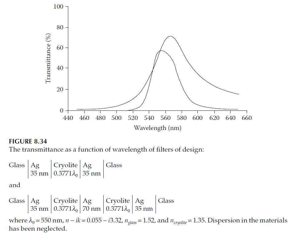
For the metal layer, we choose an arbitrary thickness of 35 nm. A single-cavity filter structure is then:
– Glass
– Ag (35 nm)
– Cryolite (0.3771 waves)
– Ag (35 nm)
– Glass
In this design, the silver thickness is quoted as geometrical thickness, and the cryolite thickness is quoted as optical thickness. A two-cavity filter doubles this structure:
– Glass
– Ag (35 nm)
– Cryolite (0.3771 waves)
– Ag (70 nm)
– Cryolite (0.3771 waves)
– Ag (35 nm)
– Glass
Performance
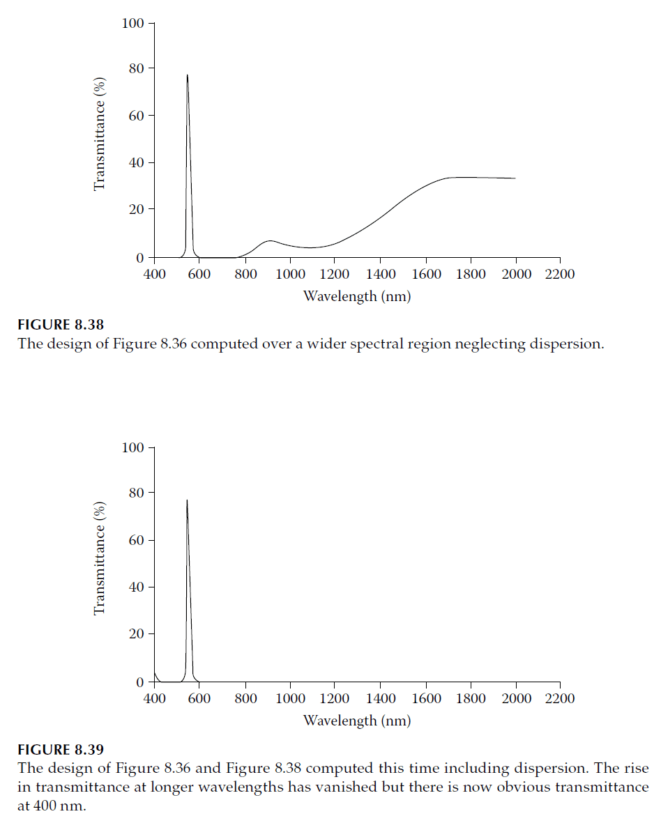
The transmittance curves for these filters are shown in Figure 8.34. The peaks are slightly displaced from 550 nm due to the approximations in the design procedure.
– The single cavity achieves reasonably good peak transmittance, but its triangular shape results in poor rejection at wavelengths far from the peak.
– The two-cavity filter has a better shape but reduced peak transmittance. Rejection can be improved by increasing metal thickness, though this further reduces peak transmittance.
Limitations of the Design Procedure
The design procedure described here is crude, focusing solely on centering the filter peak near the desired wavelength. Peak transmittance and bandwidth are either accepted as-is or adjusted by trying a different metal thickness. Performance is not optimized.
The limitations of this approach led Berning and Turner to develop a more refined technique for designing metal–dielectric filters. Their method emphasizes maximizing transmittance in the filter passband and introduces the concept of potential transmittance, resulting in a new type of metal–dielectric filter known as the induced-transmission filter.
1. The Induced-Transmission Filter
The primary question tackled by Berning and Turner is: “Given a specific thickness of metal in a filter, what is the maximum possible peak transmittance, and how can the filter be designed to achieve this transmittance?”
Potential Transmittance Concept
The concept of potential transmittance (\( \psi \)) was introduced and used to analyze losses in dielectric multilayers. It is defined as the ratio of the irradiance leaving the rear surface to that entering the front surface of a layer or multilayer assembly. It represents the transmittance the layer would achieve if the front surface reflectance were reduced to zero.
When the optical properties of the metal layer are fixed, its potential transmittance depends entirely on the admittance of the structure at the exit face. The maximum potential transmittance corresponds to a specific exit admittance. To achieve this transmittance, a coating can be added to the front surface to minimize reflectance to zero.
Key Characteristics
– The maximum potential transmittance is a function of the metal layer thickness.
– The design process involves determining the optimal exit admittance to maximize potential transmittance.
Design Procedure
1. Metal Layer Parameters:
Start with the optical constants of the metal layer (refractive index and extinction coefficient) at the peak wavelength.
2. Thickness Selection:
Choose a metal layer thickness. Determine the maximum potential transmittance and the matching admittance at the exit face required to achieve this transmittance.
– If a minimum acceptable figure for transmittance exists, this constrains the maximum allowable metal thickness.
3. Rear Matching Layer:
Design a dielectric assembly to achieve the correct matching admittance at the rear of the metal layer. This layer is typically deposited directly on the substrate.
4. Front Matching System:
Add a dielectric system to match the front surface of the metal–dielectric assembly to the incident medium, reducing reflectance and achieving the desired transmittance.
Passband Limitations
The matching admittances for the metal layer are optimized for a limited spectral region. Outside this region, the performance of the dielectric stacks degrades rapidly. This characteristic defines the limits of the filter’s passband.
Analytical Requirements
To proceed further, analytical expressions for both the potential transmittance and the matching admittance are necessary. These calculations involve lengthy but straightforward analysis. Once these expressions are derived, they enable the precise design of the filter layers and optimization of the passband.
This method represents a significant improvement over traditional trial-and-error approaches, enabling more efficient design of metal–dielectric filters with enhanced performance characteristics.
1.1 Potential Transmittance
This section focuses on calculating the potential transmittance (\( \psi \)) of a system with a single absorbing layer, the metal. The potential transmittance is linked to the characteristic matrix of the assembly.
Characteristic Matrix Representation
For the system, the characteristic matrix relates the field components as:
\[
\begin{bmatrix} B \\ C \end{bmatrix} = [M] \begin{bmatrix} 1 \\ Y_e \end{bmatrix}
\]
where:
– \( [M] \) is the characteristic matrix of the metal layer.
– \( Y_e = X + iZ \) is the complex admittance of the terminating structure, with real part \( X \) and imaginary part \( Z \).
The potential transmittance (\( \psi \)) is given by:
\[
\psi = \frac{\text{Re}(Y_e)}{\text{Re}(B/C^*)}
\tag{8.81}
\]
Phase Thickness and Complex Admittance
The characteristic matrix of the metal layer is expressed using its optical properties:
– \( y = n – ik \) is the complex refractive index of the metal.
– The phase thickness \( \delta \) is:
\[
\delta = \frac{2\pi}{\lambda} (n – ik)d = \alpha – i\beta
\]
where:
– \( \alpha = \frac{2\pi}{\lambda}nd \) is the real component.
– \( \beta = \frac{2\pi}{\lambda}kd \) is the imaginary component.
Field Components
Using the characteristic matrix, the relationship between \( B \) and \( C \) is:
\[
\begin{bmatrix} B \\ C \end{bmatrix} =
\frac{i}{y}
\begin{bmatrix}
\cos \delta & i \sin \delta \\
i \sin \delta & \cos \delta
\end{bmatrix}
\begin{bmatrix} 1 \\ X + iZ \end{bmatrix}
\]
This yields:
\[
B = \cos \delta + i \sin \delta (X + iZ)
\]
\[
C = i \sin \delta + \cos \delta (X + iZ)
\]
Simplifying \( B/C^* \)
To calculate \( \text{Re}(B/C^*) \), the following terms are expanded and simplified:
1. First Term: \( -iy^* \cos \delta \sin \delta \)
The real part is:
\[
\text{Re}(-iy^* \cos \delta \sin \delta) = n \sinh \beta \cosh \beta + k \sin \alpha \cos \alpha
\]
2. Second Term: \( \sin^2 \delta (y^* X + iZ) / (yy^*) \)
Simplifies to:
\[
\text{Re}\left[\frac{\sin^2 \delta}{y y^*}\right] =
\frac{X}{n^2 + k^2}\left(n^2 \sin^2 \alpha \cosh^2 \beta + k^2 \cos^2 \alpha \sinh^2 \beta\right)
\]
3. Third Term: \( i \sin \delta \cos \delta (X – iZ) / (yy^*) \)
The real part is:
\[
\text{Re}\left[\frac{i \sin \delta \cos \delta}{y y^*}(X – iZ)\right] = \frac{XZ}{n^2 + k^2}\left(\sinh \beta \cosh \beta – \sin \alpha \cos \alpha\right)
\]
Final Expression for Potential Transmittance
Combining the terms, the potential transmittance is:
\[
\psi = \frac{\left(n^2 \sinh^2 \beta + k^2 \sin^2 \alpha + 2nkZ\right)}{n^2 + k^2}
+ \frac{\left(\cos^2 \alpha \sinh^2 \beta + \sin^2 \alpha \cosh^2 \beta\right) X}{n^2 + k^2}
\]
This expression establishes the relationship between the optical properties, layer thickness, and maximum potential transmittance. It provides a foundation for optimizing metal–dielectric filter design.
1.2 Optimum Exit Admittance
To determine the optimum exit admittance, we analyze the potential transmittance equation. From Equation 8.82, the potential transmittance \( \psi \) can be rewritten as:
\[
\frac{1}{\psi} = p – \frac{nkZ}{(X + n^2 + k^2)} + \frac{q}{X} + \frac{r}{X^2} + \frac{sX + sZ^2}{(X^2 + n^2 + k^2)}
\tag{8.83}
\]
where:
– \( p, q, r, s \) are shorthand for terms derived from Equation 8.82.
Finding the Optimum
The potential transmittance \( \psi \) is always positive and well-behaved. For an extremum in \( \psi \), we can equivalently find the extrema of \( 1/\psi \). The optimum exit admittance satisfies the conditions:
\[
\frac{\partial}{\partial X}\left(\frac{1}{\psi}\right) = 0 \quad \text{and} \quad \frac{\partial}{\partial Z}\left(\frac{1}{\psi}\right) = 0
\]
These yield the equations:
1. For \( X \):
\[
p – \frac{nkZ}{(X^2 + n^2 + k^2)} + \frac{q}{X^2} – \frac{2r}{X^3} + \frac{s}{(X^2 + n^2 + k^2)} – \frac{2sX}{(X^2 + n^2 + k^2)^2} = 0
\tag{8.84}
\]
2. For \( Z \):
\[
p – \frac{nk}{(X^2 + n^2 + k^2)} + \frac{sZ}{(X^2 + n^2 + k^2)} = 0
\tag{8.85}
\]
From Equation 8.85, solve for \( Z \):
\[
Z = \frac{nkp}{s}
\]
Substitute this result into **Equation 8.84** to solve for \( X \):
\[
X = \frac{r(n^2 + k^2)}{s} – \frac{n^2k^2p^2}{s^2} + n^2 + k^2
\]
Simplified Expressions for \( X \) and \( Z \)
Using the expressions for \( p, q, r, s \) from **Equation 8.82**, the results are:
\[
X = \frac{(n^2 + k^2)(\sinh^2 \beta + \sin^2 \alpha) + 2nk(\sinh \beta \cosh \beta – \sin \alpha \cos \alpha)}{(n^2 + k^2) + (\sinh^2 \beta – \sin^2 \alpha)}
\tag{8.86}
\]
\[
Z = \frac{nk}{(n^2 + k^2)}\left(\sinh^2 \beta + \sin^2 \alpha – 2\sinh \beta \cosh \beta\right)
\tag{8.87}
\]
Limiting Behavior
For large \( \beta \) (thicker layers or higher absorption):
– \( X \to n \)
– \( Z \to k \)
Thus, the exit admittance approaches:
\[
Y_e \to n + ik
\]
This result implies that for large absorption, the exit admittance matches the complex refractive index of the metal layer (\( y^* \)).
1.3 Maximum Potential Transmittance
The maximum potential transmittance (\( \psi_{\text{max}} \)) is obtained by substituting the optimum values of \( X \) and \( Z \), derived from Equations 8.86 and 8.87, into the general expression for potential transmittance (Equation 8.82):
\[
\psi = \frac{n^2 \sinh^2 \beta + k^2 \sin^2 \alpha + 2nkZ}{n^2 + k^2}
+ \frac{\cos^2 \alpha \sinh^2 \beta + \sin^2 \alpha \cosh^2 \beta}{n^2 + k^2} X
+ \frac{Z^2}{n^2 + k^2}
\]
This process involves:
1. Calculating \( X \) and \( Z \) using:
– \( X \) from Equation 8.86.
– \( Z \) from Equation 8.87.
2. Substituting \( X \) and \( Z \) back into the transmittance equation to compute \( \psi_{\text{max}} \).
Computational Approach
Due to the complexity of the expressions for \( X \), \( Z \), and \( \psi \), it is impractical to solve for \( \psi_{\text{max}} \) purely analytically. Instead, numerical computation using a calculator or computer is the most efficient approach.
Summary
While the framework is analytically defined, the actual computation of \( \psi_{\text{max}} \) relies on substituting the optimum values of \( X \) and \( Z \) into the potential transmittance formula. This method ensures precise results while bypassing unnecessary manual algebraic manipulation.
1.4 Matching Stack
The goal of a matching stack is to construct an assembly of dielectric layers that, when deposited on a substrate, achieve an equivalent admittance of:
\[
Y = X + iZ
\]
This design ensures the desired admittance transformation for efficient performance of the filter.
Diagrammatic Illustration
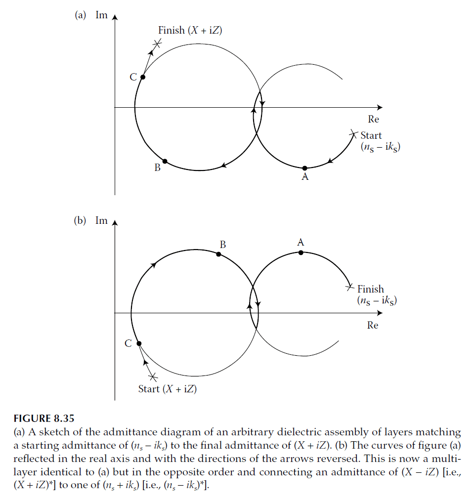
Figure 8.35 illustrates the process:
– The substrate with admittance \( n_s – i k_s \) is coated with dielectric layers, yielding a terminating equivalent admittance of \( X + iZ \).
– By reflecting this design along the \( x \)-axis and reversing the direction of the layer order:
– A new configuration (e.g., from \( ABC \) to \( CBA \)) matches the starting admittance \( X – iZ \) into the terminal admittance \( n_s + i k_s \), the complex conjugate of the substrate index.
For most practical cases:
– Substrates are assumed to have real admittance (\( k_s = 0 \)).
– The problem simplifies to matching \( X – iZ \) into \( n_s \), which is more straightforward.
Matching Strategy
1. Phase-Matching Dielectric Layer:
– To simplify the problem, a dielectric layer is added to convert the complex admittance \( X – iZ \) into a real admittance (\( \mu \)).
– This layer is designed with an optical thickness \( D \) given by:
\[
D = \frac{1}{4} \arctan\left(\frac{Z}{n_f^2 – X^2 – Z^2}\right)
\tag{8.88}
\]
where:
– \( n_f \) is the characteristic admittance of the film.
– The tangent is taken in the first or second quadrant.
– The resulting real admittance \( \mu \) is calculated as:
\[
\mu = \frac{X^2 n_f^2 + Z^2 + (n_f^2 – X^2 – Z^2)^2}{X^2 + Z^2}
\tag{8.89}
\]
2. Quarter-Wave Stack:
– After the phase-matching layer, a quarter-wave stack is added to match \( \mu \) to \( n_s \), the substrate admittance.
– The quarter-wave stack alternates between high- and low-index layers, starting with a low-index layer if the substrate admittance is greater than unity.
– The precise number of layers is determined by trial and error to achieve optimal matching.
Final Matching Design
– Matching Front Surface:
The equivalent admittance at the front surface of the metal layer is calculated. A second matching stack is designed to transform this admittance to match the incident medium (usually air, with an admittance of 1).
– Simplification Notes:
There are infinite possible solutions for matching stacks, but the described approach is straightforward and practical. It relies on transforming the complex admittance into a real value before implementing the quarter-wave stack.
Summary
The matching stack consists of two parts:
1. A phase-matching layer to convert the complex admittance \( X – iZ \) into a real admittance \( \mu \).
2. A quarter-wave stack to match \( \mu \) to the substrate admittance \( n_s \).
This layered approach ensures efficient matching, improving the filter’s optical performance. The detailed calculations and iterative adjustments are essential steps to refine the design and achieve the desired results.
1.5 Front Surface Equivalent Admittance
If the admittance at the exit surface of the metal layer is the optimum value (\( X + iZ \)) as derived in Equations 8.86 and 8.87, then the equivalent admittance presented at the front surface of the metal layer is simply the complex conjugate:
\[
Y = X – iZ
\]
Logical Justification
The proof for this relationship is not particularly difficult but involves detailed mathematical analysis. Instead of deriving it analytically, the following logical justification illustrates the principle:
1. Symmetry of Transmittance:
Consider a filter with a single metal layer sandwiched between dielectric matching stacks.
– Assume the admittance at the rear of the metal layer is \( X + iZ \), and the equivalent admittance at the front surface is \( \xi + i\eta \).
– Suppose the filter’s transmittance equals the **maximum potential transmittance**, and the front surface is perfectly matched to the incident medium.
2. Reversibility of Light:
The transmittance of the filter is independent of the direction of light propagation.
– If the filter is flipped, the transmitted light propagates in the opposite direction.
– The admittance at the new exit face of the metal layer (formerly the input face) must be \( X + iZ \) to maintain the maximum potential transmittance.
3. Complex Conjugate Relationship:
Since the dielectric layers and the surrounding medium are lossless and symmetric:
– The admittance at the new input face (formerly the exit face) must be the complex conjugate of \( \xi + i\eta \), i.e., \( \xi – i\eta \).
– Therefore, \( \xi + i\eta = X – iZ \).
This symmetry ensures that the equivalent admittance at the front surface of the metal layer is \( X – iZ \).
Matching Procedure
The process for matching the front surface to the incident medium is identical to that for the rear surface:
– A phase-matching layer can be added to convert \( X – iZ \) into a real admittance.
– A quarter-wave stack can then be used to match the real admittance to the surrounding medium.
If the incident medium is the same as the rear exit medium (e.g., in a cemented filter assembly), the front dielectric section can be an exact replica of the rear section.
Summary
The equivalent admittance at the front surface of the metal layer is \( X – iZ \), the complex conjugate of the admittance at the rear surface. This property simplifies the design, allowing the front dielectric matching section to mirror the rear if the surrounding media are identical.
2. Examples of Filter Designs
This section explores specific designs for metal-dielectric filters, using silver as the metal layer. The optical constants for silver are taken as \( n = 0.055 \) and \( k = 3.32 \) at a wavelength of \( \lambda = 550 \, \text{nm} \) [33]. The filter uses dielectric materials with refractive indices \( n_L = 1.35 \) (cryolite) and \( n_H = 2.35 \) (zinc sulfide). The substrate and incident medium are glass with \( n = 1.52 \).
Filter Design with Silver
1. Metal Layer Parameters:
Thickness of silver = 70 nm.
Calculating phase thickness parameters for silver:
\[
\alpha = \frac{2\pi n d}{\lambda} = 0.04398, \quad \beta = \frac{2\pi k d}{\lambda} = 2.6549
\]
Using Equations 8.86 and 8.87:
\[
X + iZ = 0.4572 + i3.4693
\]
Substituting into Equation 8.82, the potential transmittance:
\[
\psi = 80.50\%
\]
2. Phase-Matching Layer Design:
A low-index layer (\( n = 1.35 \)) is selected as the phase-matching layer.
Using Equation 8.88, the optical thickness:
\[
D = 0.19174 \, \text{full waves}
\]
Using Equation 8.89, the real admittance after phase matching:
\[
\mu = 0.05934
\]
3. Quarter-Wave Stack Matching:
Match \( \mu \) to the substrate admittance (\( n_s = 1.52 \)). Starting with a low-index quarter-wave layer, compute the matching sequence:
\[
n_L^2 / \mu, \quad n_H^2 / n_L^2 / \mu, \quad n_L^4 / n_H^2 / \mu, \quad \dots
\]
After trial and error, the optimal configuration involves three layers of each type:
\[
n_H^6 / n_L^6 = 1.6511
\]
Loss at the substrate interface = 0.2%.
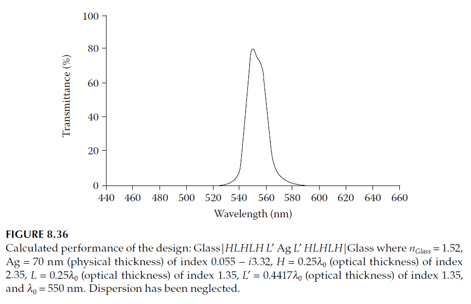
4. Final Design:
Combine the matching stack and phase-matching layer into the structure:
\[
\text{Glass}|HLHLHL L′ \, \text{Ag} \, L′ HLHLH| \text{Glass}
\]
where:
\[
L′ = 0.44174 \, \text{full waves} \, \text{(optical thickness)}, \quad H, L = 0.25 \, \text{full waves}
\]
Performance, shown in Figure 8.36, predicts the peak at 550 nm with \( \psi \approx 80.50\%\).
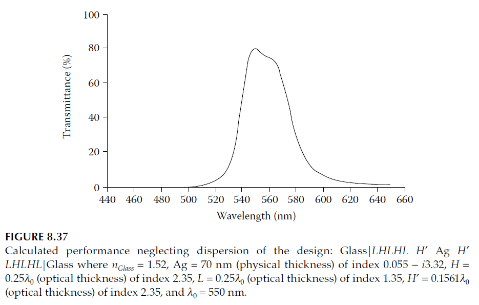
Alternative High-Index Matching Layer
If a high-index (\( n = 2.35 \)) layer is selected:
– Optical Thickness:
\[
D = 0.1561 \, \text{full waves}
\]
– Real Admittance:
\[
\mu = 0.1426
\]
Matching options involve different sequences of layers. The optimal configuration minimizes loss to 0.2%, leading to:
\[
\text{Glass}|LHLHLH′ \, \text{Ag} \, H′ LHLHL| \text{Glass}
\]
where \( H′ = 0.1561 \, \text{full waves} \). Performance is shown in Figure 8.37.
Extended Designs
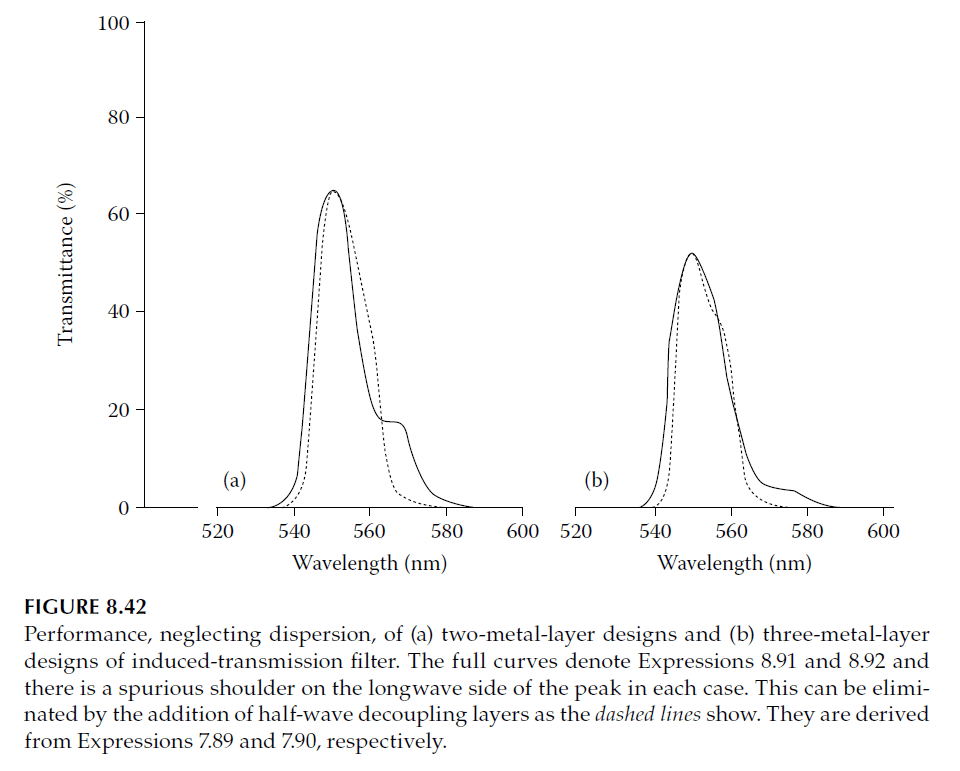
1. Two-Metal Layer Filter:
Adding another metal layer with the same thickness (70 nm) improves rejection. Use a dielectric layer twice the thickness of the phase-matching layer:
\[
L′′′ = 2 \times 0.19174 = 0.38348 \, \text{full waves}
\]
Design:
\[
\text{Glass}|HLHLH L′ \, \text{Ag} \, L′′′ \text{Ag} \, L′′′ HLHLH| \text{Glass}
\]
Performance predicts \( \psi^2 = 64.8\% \).
2. Three-Metal Layer Filter:
Add a third metal layer, using the same principles:
\[
\psi^3 = 52.17\%
\]
Design:
\[
\text{Glass}|HLHLH L′ \, \text{Ag} \, L′′′ \text{Ag} \, L′′′ \text{Ag} \, L′ HLHLH| \text{Glass}
\]
Performance (logarithmic scale) is shown in Figure 8.41, demonstrating improved rejection.
Improving Passband Shape
Adding a half-wave layer to \( L′′′ \):
\[
L_{IV} = 0.5 + 0.38348 = 0.88348 \, \text{full waves}
\]
Revised designs:
\[
\text{Glass}|HLHLH L′ \, \text{Ag} \, L_{IV} \, \text{Ag} \, L_{IV} HLHLH| \text{Glass}
\]
Performance (Figure 8.42) shows elimination of longwave humps.
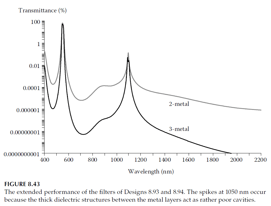
Design Notes
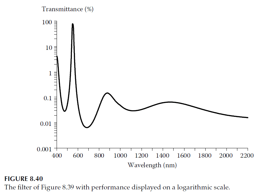
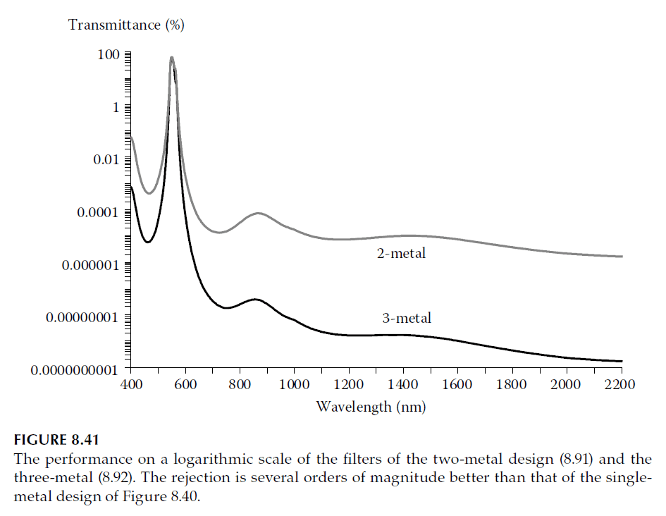
– Dispersion: Performance improves when considering dispersion effects of silver. Longwave rejection becomes significant, as shown in Figures 8.39 and 8.43.
– Applications:
– Filters with lower rejection are suited for general-purpose use.
– Filters with higher rejection are ideal for suppressing sidebands in all-dielectric filters.
– Practical Manufacturing:
– Trial-and-error optimization of silver thickness is recommended.
– For ultraviolet filters, materials like aluminum perform less effectively than silver in the visible region.