1. Electrode Films for Schottky-Barrier Photodiodes
A simple diode photodetector consists of a metal layer deposited over a semiconductor forming a Schottky barrier. High quantum efficiency can be achieved. The incident light passes through the metal layer into the depletion layer of the diode, where it creates electron-hole pairs. The metal contact layer must transmit the incident light, and since it has intrinsically high reflectance, it must be coated to reduce its reflection loss.
We present a simple approach to designing a combination of electrode and antireflection coating. Several researchers have contributed to this area, with Schneider providing perhaps the most complete analytical approach.
The substrate for the thin films is the semiconducting part of the diode, and its optical admittance is fixed. The metal layer is deposited directly over the semiconductor (in some cases, with a very thin insulating layer that has negligible optical interference effects), meaning the potential transmittance is entirely determined by the thickness of the metal. Maximizing transmittance relies on reducing reflectance to zero.
For example, consider a gold electrode layer deposited on silicon at a wavelength of 700 nm. The optical constants are assumed to be:
- Gold: \( 0.131 – i3.842 \)
- Silicon: \( 3.92 – i0.05 \)
The optical constants of silver and copper are similar to gold at this wavelength, so the results apply nearly equally to these alternative metals.
The admittance locus of a single gold film on silicon is shown in Figure 15.24. An antireflection coating must bridge the gap between the appropriate point on the metal locus and the point \((1, 0)\), corresponding to the admittance of air.
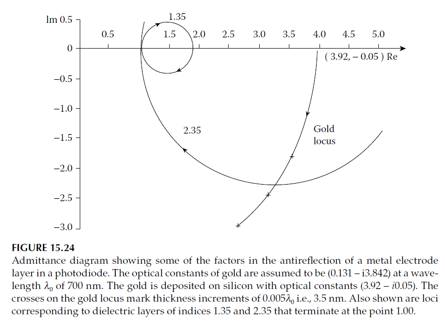
We assume the maximum and minimum values of dielectric layer admittance available for antireflection coatings are 2.35 and 1.35, respectively. Using these values, two circles can be added to the admittance diagram, passing through the point \((1, 0)\).
These correspond to admittance loci of dielectric materials with characteristic admittances of 2.35 and 1.35. The loci define the limits of a region in the complex plane. If a metal locus ends within this region, it is possible to find a dielectric overcoat with admittance between 1.35 and 2.35 that, when correctly chosen in thickness, will reduce reflectance to zero.
From the diagram, the thicker the metal film, the higher the admittance of the antireflection coating must be. Once the metal locus extends beyond this region, a single dielectric layer is insufficient, and a multilayer coating becomes necessary. Multilayer coatings or single absorbing layers (less practical in this case as they reduce transmittance) may then be required.
For simplicity, we limit the design to a single dielectric layer, using the highest available index of 2.35.
Design and Calculation
The design process involves determining the thicknesses of the metal and dielectric corresponding to the trajectories:
1. Between the substrate and the point of intersection.
2. Between the point of intersection and the point \((1, 0)\) in Figure 15.24.
The points marked along the metal locus correspond to intervals of \(0.005\lambda_0\) in geometrical thickness, equivalent to intervals of 3.5 nm. Visual estimation suggests a thickness of \(0.013\lambda_0\) at the point of intersection, with more accurate calculations yielding:
- Metal thickness: \(0.0133\lambda_0\) (\(9.3 \, \text{nm}\)).
- Dielectric layer thickness: Optical thickness of approximately \(0.186\lambda_0\), falling between an eighth-wave and a quarter-wave.
Performance and Observations
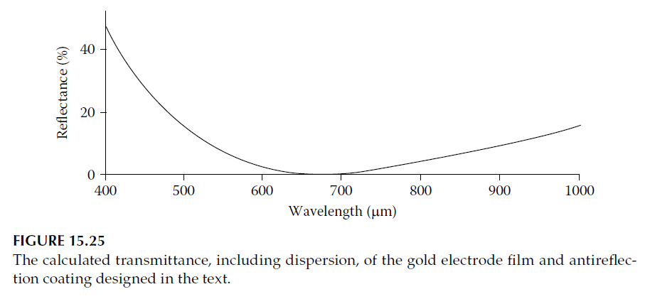
The calculated performance of this coating is illustrated in Figure 15.25. Although the metal film’s thickness is small, meaning the optical constants measured on thicker films might not apply without corrections, the curve’s form and the coating’s basic principles are as discussed.
2. Spectrally Selective Coatings for Photothermal Solar Energy Conversion
Coatings for solar energy applications represent an extensive field of study. These coatings have been discussed in detail by Hahn and Seraphin. This section focuses on a limited range of coatings based on antireflection coatings over metal layers, which share similarities with the electrode films discussed earlier.
Solar Absorber Challenges and Solutions
Solar absorbers operating at elevated temperatures lose heat via radiation unless steps are taken to reduce their emittance in the infrared region. At the same time, efficient operation requires high solar absorptance in the visible and near-infrared regions. The optimal coating achieves a sharp transition from absorption to reflection at a wavelength that varies with the absorber’s operating temperature.
One approach involves starting with a thick metal film or substrate and applying an antireflection coating effective in the visible spectrum but ineffective in the infrared. This results in high reflectance at longer wavelengths, reducing thermal emittance.
In this case, reflectance reduction is the primary goal. Transmittance is not critical since unabsorbed energy in the coating is absorbed in the substrate. This enables the inclusion of absorbing layers in the antireflection coating design.
Semiconducting Layer with Antireflection Coating
A practical approach employs a semiconducting layer over a metal. In the infrared, beyond the semiconductor’s intrinsic edge, the layer becomes transparent, allowing the underlying metal’s reflectance to dominate. In the visible and near-infrared, the semiconductor absorbs enough to suppress metallic reflectance. Completing the design involves adding an antireflection coating to reduce the front-face reflectance of the semiconductor.
- Metal Dominance in the Infrared: The metal’s high \(k/n\) ratio ensures minimal influence from the semiconductor’s high index in its transparent region.
- Silver as the Preferred Metal: Silver, with its favorable optical constants, is ideal but suffers from stability issues at elevated temperatures. To address this, chromium oxide (Cr₂O₃) layers stabilize silver by acting as diffusion inhibitors.
Silicon-Based Coating Design
Silicon films are deposited by chemical vapor deposition, breaking silicon-hydrogen bonds in silane gas over heated substrates. Oxygen or nitrogen added to the gas stream forms silicon oxide or nitride antireflection coatings, which can withstand temperatures exceeding 600°C.
1. Silicon Layer Thickness:
- Visible absorption should mask the silver without introducing interference effects that reduce infrared reflectance and increase emittance.
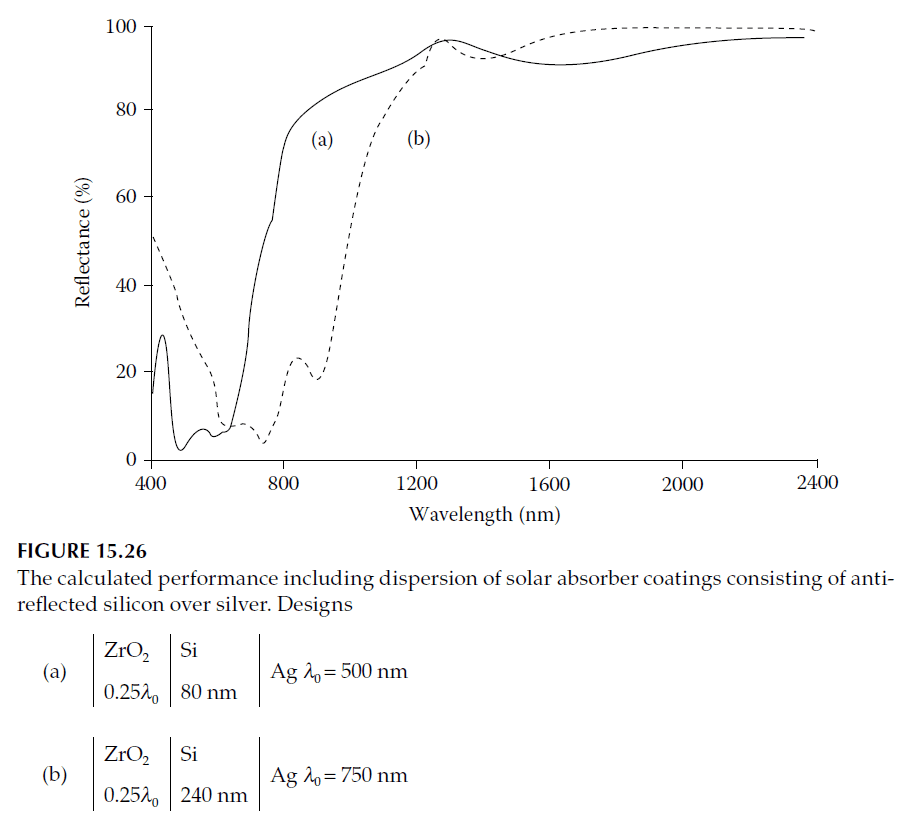
- Light attenuation follows \( \exp(-4\pi k d / \lambda) \). For a reduction to 0.05 at 500 nm (\( n = 4.3 – i0.74 \)), the thickness \( d \) for a round trip is \( 160 \, \text{nm} \), giving a film thickness of \( 80 \, \text{nm} \).
2. Antireflection Coating:
- To reduce front-surface reflectance, a homogeneous film with an admittance of 2.0 and a quarter-wave thickness at 500 nm is used.
- Example: Zirconium dioxide (\( n = 2.07 \)).
The performance of this coating is shown in Figure 15.26. An additional dip at 600 nm arises from silicon thickness and interference effects. The reflectance trough can shift to a longer wavelength (e.g., 750 nm) by adjusting the design.
Alternative Designs Using Metal Layers
Metal layers can also function as part of an antireflection coating for high-efficiency metals like silver. Dielectric layers alone require many quarter-wave pairs to achieve zero reflectance, as the admittance locus progresses incrementally with each pair.
A metal layer offers a different trajectory, cutting across dielectric loci, bridging gaps more effectively. The design can use a metal like chromium for its flatter trajectory and broader spectral characteristics, offering additional dielectric layer protection.
1. Example Design:
– Wavelength: 500 nm.
– Materials and Constants:
- Silver: \( 0.05 – i2.87 \)
- Aluminum oxide: \( n = 1.67 \)
- Chromium: \( 2.86 – i4.11 \)
2. Performance:
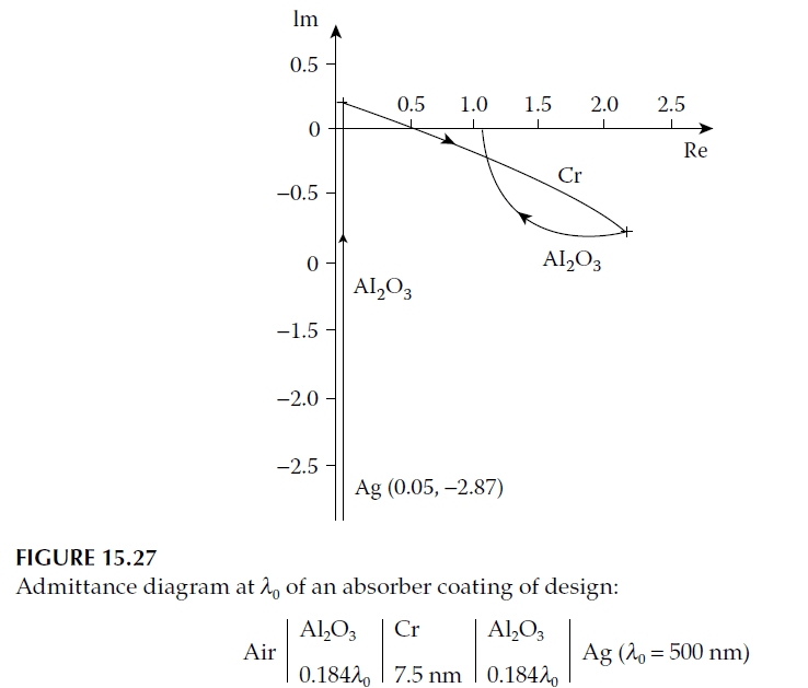
- Figure 15.27: Admittance diagram for a coating where the chromium layer bridges dielectric gaps.
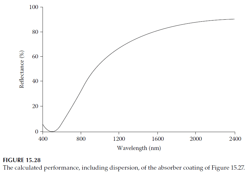
- Figure 15.28: Characteristic curve of the coating.
The chromium layer’s lower \(k/n\) ratio results in flatter trajectories, making the design less sensitive to wavelength changes. This arrangement ensures the coating terminates near \((1,0)\) across varying wavelengths. While this example was not refined, significant performance improvements are possible with further optimization.
Shifting Reflectance Minima and Practical Considerations
The reflectance minimum can be shifted to longer wavelengths by repeating the design process with appropriate values of the optical constants. This adjustment achieves the desired zero reflectance; however, at shorter wavelengths, the dielectric loci diverge further from the ideal. In such cases, the chromium layer becomes unable to bridge the gap between them, resulting in a peak of high reflectance.
At even shorter wavelengths, a second-order minimum arises. This occurs when the dielectric layers complete a full revolution in the admittance diagram and return to the vicinity of the ideal position. For the idealized values used in these calculations, the central peak of high reflectance is very pronounced.
Practical coatings, as described by Hahn and Seraphin, also exhibit this double-minimum behavior, but the central maximum is much less prominent. The most likely explanation is that real-world layers exhibit greater losses than assumed in theoretical models.
Thin chromium layers, in particular, are unlikely to possess ideal optical constants. High losses would cause the loci to spiral inward toward the center of the admittance diagram, thereby reducing wavelength sensitivity.
High-Temperature Stability and Practical Challenges
The major challenges associated with these coatings are not related to design but to achieving high-temperature stability. Spectrally selective solar absorbers are economically viable only when used to produce high temperatures. They are advantageous over conventional spectrally flat black absorbing surfaces, which can be produced at significantly lower costs, only at elevated temperatures.
1. Operational Environment:
These coatings are typically used under vacuum to eliminate heat losses from gas conduction. Under such conditions, the primary degradation mechanism is diffusion within the coatings.
2. Material Challenges:
- Silver: Prone to agglomeration at high temperatures, leading to shifts in optical properties and reduced performance.
- Chromium Oxide Diffusion Barriers: These are incorporated into coatings to inhibit diffusion and agglomeration of components without adversely affecting optical properties.
3. Performance and Longevity:
The development of diffusion barriers like chromium oxide has significantly improved the lifetime of these coatings at high temperatures. Achievements in this field are notable, and further details can be found in Hahn and Seraphin.
3. Heat-Reflecting Metal–Dielectric Coatings
Heat-reflecting filters have several valuable applications. For instance, a spectrally flat solar absorber can be paired with such a filter to create a spectrally selective absorber. A simple band-pass filter with the desired characteristics can be constructed using a single metal layer sandwiched between two dielectric matching layers. This filter shares some similarities with the induced transmission filter, though the maximum theoretical transmittance is rarely achieved.
Design Approach
One design technique uses the admittance diagram, which we illustrate with an example:
- Substrate and Incident Medium:
A glass substrate with an incident medium of air or vacuum. - Metal Layer:
Silver, with optical constants of \( 0.06 – i3.75 \) at 600 nm, is used as the metal layer. - Dielectric Layers:
A dielectric material with a refractive index of 2.35 is chosen. Zinc sulfide (ZnS) is a suitable candidate, but coatings using refractory oxides are more durable and stable.
Admittance Diagram and Zero Reflectance
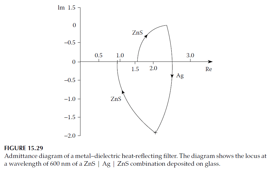
Figure 15.29 shows the admittance diagram for this design. One dielectric locus begins at the substrate, while a second terminates at \((1,0)\), corresponding to the incident medium. For the complete coating to achieve zero reflectance, the remaining layers must bridge the gap between these two loci.
- Role of the Metal Layer:
The metal layer bridges this gap, with its optical constants influencing the points of intersection with the dielectric loci. - Layer Adjustments:
Increasing the metal thickness without sacrificing zero reflectance requires higher refractive indices for the dielectric layers. Alternatively, inserting a low-index quarter-wave layer next to the substrate can move the starting point of the next high-index dielectric layer further along the real axis, allowing a thicker metal layer.
Example Design
The final three-layer design is as follows:
| Layer | Material | Index | Thickness |
|---|---|---|---|
| Air | |||
| Dielectric | Zinc sulfide (ZnS) | 2.35 | \(0.146\lambda_0\) |
| Metal | Silver (Ag) | \(0.06−i3.75\) | 15 nm |
| Dielectric | Zinc sulfide (ZnS) | 2.35 | \(0.141\lambda_0\) |
| Substrate | Glass | 1.52 | \(\lambda_0 = 600\text{ nm}\) |
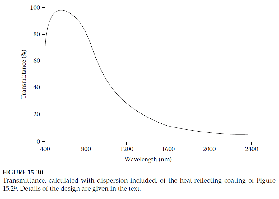
The performance of this coating is shown in Figure 15.30.
Observations and Performance
- Infrared Reflectance:
The steep fall in performance toward the infrared is partially due to the decreased matching efficiency. However, metals exhibit significant dispersion in this range. The value of \( (2\pi kd/\lambda) \) remains high due to increasing \( k \), which lengthens the locus in the infrared and induces a considerable rise in reflectance. - Alternative Materials:
Coatings based on other metals with high infrared reflectance, such as gold, paired with high-index dielectric materials like bismuth oxide, have also been successful.
Protective Measures for Silver
Silver oxidizes when exposed to air, necessitating protective diffusion barrier layers. Commonly used barriers include nickel, chromium, and titanium. These protective metals are believed to oxidize in situ, creating a tightly packed oxide layer that serves as an effective diffusion barrier. These thin oxide layers have minimal optical impact.
