A variety of processes are employed to deposit optical coatings, the most common being physical vapor deposition (PVD), which typically occurs under vacuum. In PVD, thin films condense directly in the solid phase from the vapor. While the term “physical” distinguishes it from “chemical,” chemical reactions may still play a role in film formation. However, chemical vapor deposition (CVD) refers specifically to techniques where a chemical reaction between precursors forms the film, resulting in properties significantly different from the starting materials.
Physical Vapor Deposition (PVD)
PVD processes can be classified based on the methods of vapor generation and the energy involved in film deposition and growth. The main types include:
Thermal Evaporation
– The material to be deposited (evaporant) is heated to its vaporization temperature.
– The vapor condenses as a solid film on substrates maintained below the evaporant’s freezing point.
– Molecules travel in nearly straight lines between the source and substrate, with deposition following laws similar to those of illumination.
– Advantages: Simplicity, flexibility, low cost, and widespread availability of systems.
– Shortcomings: Films often have poor microstructure, limiting their performance for specialized applications.
Sputtering
– A target is bombarded with energetic particles (usually ions), ejecting atoms and molecules to form the vapor.
– Sputtered particles have much higher energy than those from thermal evaporation, resulting in denser, more compact films.
– Sputtering is part of a broader category known as energetic processes, which supply additional energy to the film through direct particle bombardment.
Chemical Vapor Deposition (CVD)
CVD is increasingly applied to optical coatings. In CVD, chemical reactions between starting materials (precursors) form the coating material. These reactions can be triggered by various methods, the most common being plasma-enhanced CVD, which uses an electrically induced plasma.
Comparison with PVD
– Advantages: CVD can produce coatings that challenge PVD methods and is well-suited for large-scale production of similar components.
– Limitations: CVD requires reactors tailored to specific products, reducing flexibility compared to PVD.
– Complementary Role: CVD is not a direct competitor to PVD but complements it, especially for complex coatings.
Other Deposition Methods
Historically, thin-film production began with techniques like:
1. Chemical etching of glass (e.g., Fraunhofer’s work).
2. Deposition from solutions.
Other techniques occasionally employed include:
– Anodic oxidation (e.g., protective coatings on aluminum).
– Spraying materials as solutions, vapors, or substances convertible into desired films.
– Polymerization of monomers deposited via condensation or solution.
– Extrusion of self-supporting thin-film multilayers.
—
1. Thermal Evaporation
In thermal evaporation, the vapor is produced by heating the material, referred to as the evaporant. Due to the reduced pressure in the chamber, the vapor is emitted in a smooth, even stream, with molecules traveling in straight lines. This allows for uniform film thickness that depends on the substrate’s position and orientation relative to the vapor source. The properties of the resulting film are broadly similar to those of the bulk material, although differences in microstructure may occur.
Ensuring good film quality requires several precautions:
– The substrate surface must be scrupulously clean.
– The vapor stream should ideally approach the substrate at near-normal incidence.
– The substrate may need to be heated to temperatures ranging from 200–300 °C (or higher) before deposition, depending on the material.
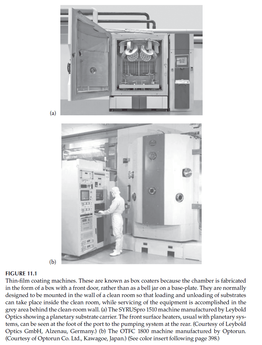
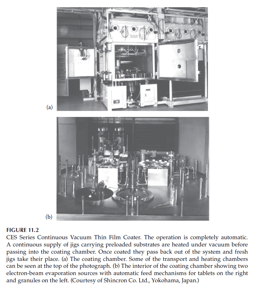
The evaporation process takes place in a sealed vacuum chamber evacuated to pressures typically around \(10^{-5} \, \text{mbar}\) (\(10^{-3} \, \text{Pa}\)). The materials are melted using various techniques, described in subsequent sections. A complete deposition system includes the vacuum chamber, pumps, pressure gauges, power supplies for heating the evaporant, thin-film thickness monitoring equipment, substrate holders and heaters, and control systems. Figures 11.1 and 11.2 show examples of modern thin-film coating machines.
A notable enhancement in thermal evaporation is ion-assisted deposition, where energetic ions bombard the growing film, compacting it through momentum transfer. The machines illustrated in Figures 11.1 and 11.2 include sources for generating these ions.
—
Heating Methods
To evaporate the material, it is placed in a crucible or boat and heated until molten, or until it sublimes, if applicable. Several methods are used:
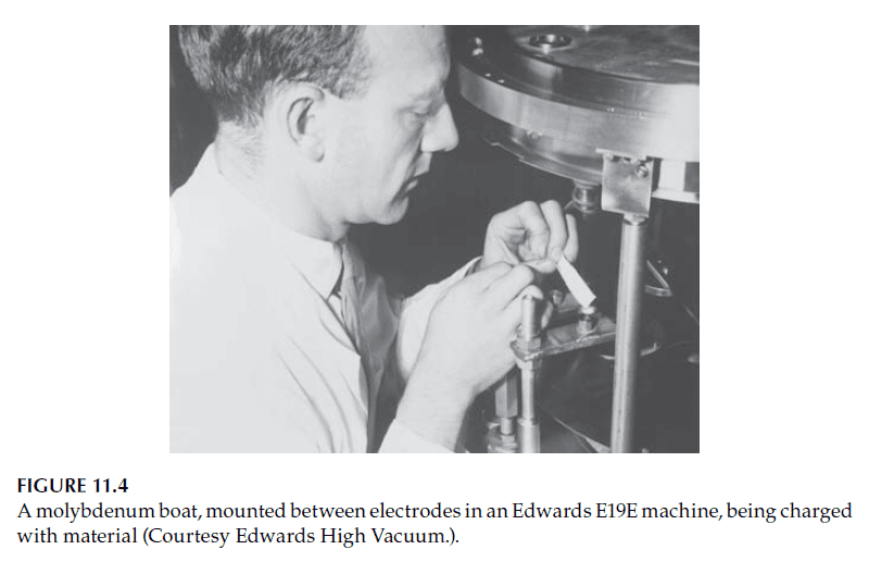
1. Resistive Heating with Boats:
– Boats made of refractory metals (e.g., tantalum, molybdenum, tungsten) act as heaters.
– High currents (several hundred amps) are passed through the boats to heat the material.
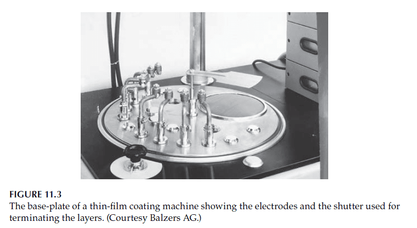
– Electrodes holding the boats are typically water-cooled to prevent damage (see Figures 11.3 and 11.4).
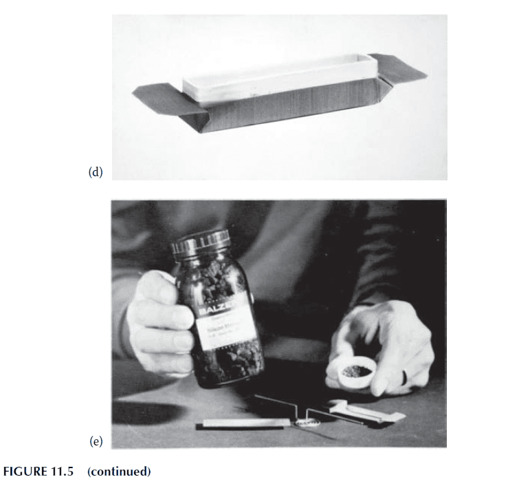
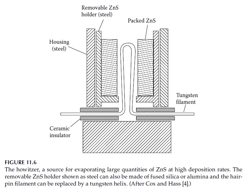
2. Crucibles for Subliming Materials:
– Materials like zinc sulfide or silicon monoxide, which sublime at lower temperatures, can be heated in alumina or fused silica crucibles using radiation from a tungsten spiral placed above the material. The “howitzer” source, shown in Figure 11.6, is an example of this type of source.
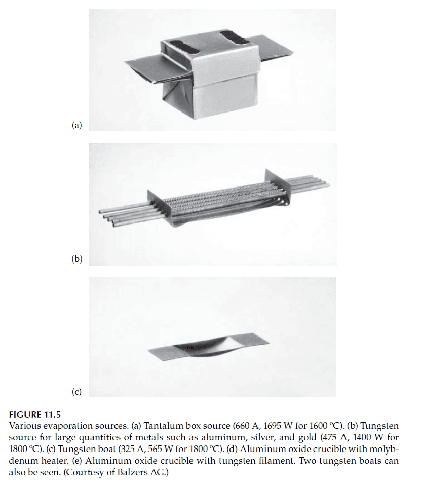
3. Graphite Boats for Reactive Materials:
– For materials like germanium that react with alumina, graphite boats are effective. These boats are easy to machine and compatible with refractory metals like copper for electrical contacts.
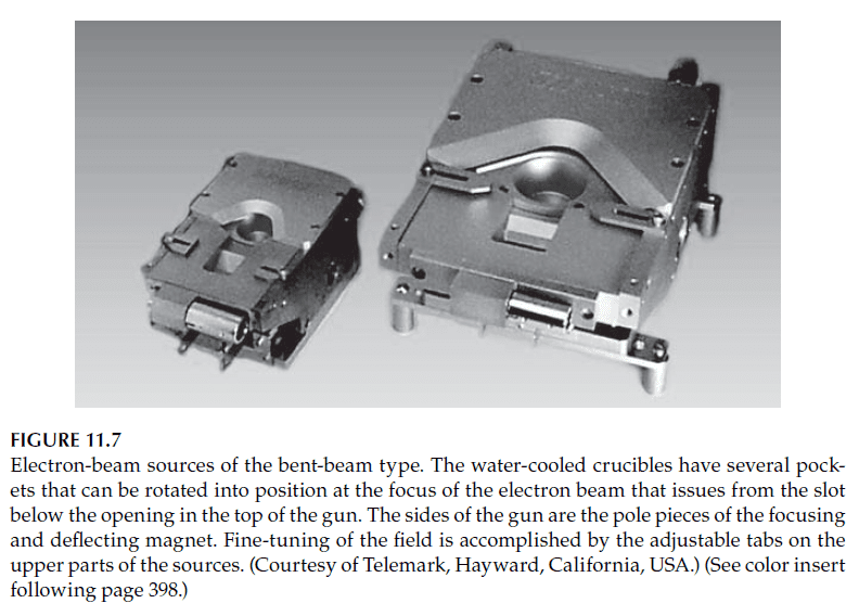
4. Electron-Beam Heating:
– A preferred method for refractory oxides and reactive materials, this technique uses an electron beam to heat and vaporize the material in a copper hearth (Figures 11.7). Electron-beam sources are versatile and can handle multiple materials using multi-pocket hearths.
—
Substrate Temperature
The temperature of the substrate influences film properties significantly:
– Higher temperatures produce denser, more stable films, typically around 300 °C for refractory oxides.
– Consistent temperature control is critical, achieved using thermocouples or infrared thermometers.
– For certain metals, like rhodium and platinum, elevated substrate temperatures improve results.
—
Load Lock Systems
Systems like the one in Figure 11.2 include load lock mechanisms to maintain the deposition chamber’s vacuum conditions while introducing or removing substrates. This minimizes contamination and stabilizes coating conditions.
—
Chamber Cleaning
Cleaning is essential due to vapor deposition on chamber walls and components:
– Shields minimize deposition on hard-to-clean areas and can be protected with disposable aluminum foil.
– Cleaning methods include mechanical (e.g., bead blasting) and chemical processes, followed by baking to remove residual fluids and particles.
—
2. Energetic Processes
Energetic processes involve higher energy levels compared to thermal evaporation, with the goal of disrupting the columnar structure and voids that commonly result in coating instability and drift. These processes leverage additional momentum to achieve denser and more stable thin films.
Sputtering
Sputtering is an established technique predating thermal evaporation. It ejects atoms or molecules from a target into the vapor phase via momentum transfer from energetic ions. The kinetic energy and momentum of ejected particles disrupt the columnar structure during film growth.
DC Planar Magnetron Sputtering
In its conventional form, sputtering employs metallic targets and a DC discharge. For optical coatings, magnetron sputtering is frequently used, where crossed electric and magnetic fields confine the discharge near the target. This allows the process to operate at lower pressures (e.g., \(0.3 \, \text{Pa}\)) compared to conventional sputtering. A schematic of a DC planar magnetron target is shown in Figure 11.8.

However, magnetron sputtering has disadvantages:
– Non-uniform Erosion: Magnetic fields concentrate erosion in specific regions, often forming a “racetrack” pattern, reducing target utilization.
– Reactive Sputtering Challenges: When producing oxides or nitrides, insulating films can form on less-eroded target regions, leading to issues such as target poisoning, arcing, and electrical instability.
Solutions to these challenges include:
1. Rotating Targets: Moving the target relative to the magnets to remove insulating layers.
2. Mid-Frequency Sputtering: Alternating target polarity at frequencies of 10–40 kHz, discharging insulating layers before damage occurs.
3. Closed-Field Magnetron Sputtering: Using multiple magnetron sources arranged to create a magnetic bottle effect, enhancing plasma uniformity around substrates.
—
Microplasma Sputtering
In this variation, magnetron sources operate in argon within a shroud to avoid poisoning. Reactive gases (e.g., oxygen or nitrogen) are introduced outside the shroud, bombarding the growing film with ions. This technique produces dense, amorphous films with high-quality optical properties.


—
Ion-Beam Sputtering
Ion-beam sputtering uses a separate chamber to generate ions that are extracted and directed toward the target (Figures 11.13 and 11.14). This method achieves:
– High film purity.
– Low optical losses (e.g., <1 ppm in multilayer reflectors). – Applicability to both insulating and conductive materials. Despite its advantages, ion-beam sputtering is slower and less suitable for large-area coatings.


—
Ion-Assisted Deposition
This process involves thermal evaporation combined with bombardment by energetic, neutralized ion beams. The additional momentum compacts the growing film, resulting in denser, more durable coatings. Kaufman-type gridded ion guns are commonly used for precise control of ion energy. Non-gridded ion sources are also gaining popularity for production applications.

—
Reactive Low-Voltage Ion Plating
This technique employs a low-voltage, high-current electron beam to ionize evaporant and reactive gases in the chamber. The ionized particles bombard the substrate, creating dense, hard, and optically pure films.


—
Radical-Assisted Sputtering (RAS)
RAS combines rotating magnetron sources with atomic oxygen or nitrogen interaction, producing films of high density and consistent quality. The lack of bombardment enhances film properties while reducing costs and enabling large-batch production. An example of an RAS machine is shown in Figure 11.18.

—
Advantages of Energetic Processes
Energetic processes offer several benefits:
– Increased Packing Density: Results in bulk-like films with higher durability and reduced moisture sensitivity.
– Improved Adhesion: Interfacial mixing enhances film adhesion.
– Reduced Tensile Stress: Leads to more stable coatings.
– Enhanced Material Reactivity: Enables deposition of compounds like nitrides that are challenging with traditional methods.
Computer modeling and experimental evidence highlight the significance of momentum over energy in achieving these effects. Applications include improved magnesium fluoride films for high-temperature oxidation resistance and enhanced hardness and corrosion resistance of metal films with dielectric overcoats.
—
3. Other Processes
Physical vapor deposition (PVD) processes are most often used for producing optical coatings. However, in the field of electronic devices, chemical vapor deposition (CVD) is the principal method for thin-film deposition, and there is increasing interest in using it for optical purposes, particularly for specialized requirements.
CVD differs from PVD in that the film material is produced by a reaction among the components of the vapor surrounding the substrates. The reaction may be:
1. Induced by the temperature of the substrates (classic thermal CVD), or
2. Plasma-induced, which is more common in optical applications.
In the CVD process, reactants or precursors are typically introduced into a carrier gas, ensuring a steady supply to the substrate’s surface. Proper dilution is critical to prevent overly rapid reactions, which can result in poorly packed and poorly adherent films often described as “snow.” Pulsed processes are often adopted to overcome these challenges, as they allow better control over the deposition rate and ensure the film is dense and adherent.
In plasma-assisted CVD (PACVD), material deposition occurs at a controlled rate, enhancing film quality. A related process, plasma polymerization, is used to deposit dense organic layers with stable optical properties, especially on curved or irregular surfaces. Unlike conventional polymerization, plasma polymerization involves energetic electrons breaking reactants into active fragments that recombine to form the deposited film. These films exhibit strong binding, making them tough, hard, and dense, with properties ranging from plastic-like to glass-like.
Typical applications include depositing silicon dioxide using precursors like tetraethoxysilane (TEOS) and oxygen. However, for plastic substrates, the process requires lower temperatures, complicating the film composition. Several silicone compounds, such as hexamethyldisiloxane (HMDSO) and methyltrimethoxysilane (MTMOS), can serve as precursors, yielding tough, abrasion-resistant coatings often used as “hard coats.” Fluorine compounds are used for hydrophobic, anti-smudge layers in antireflection coatings.
Atomic Layer Deposition (ALD)
ALD shares some similarities with CVD but involves a sequential, surface-controlled process. In ALD, the substrate is exposed to a precursor that chemisorbs onto its surface, ideally forming a monolayer. After purging, a second precursor is introduced, forming a single molecular layer of the compound. This cycle repeats to build up the desired film thickness.
Advantages of ALD include:
– Uniform film thickness on complex substrates.
– High-quality, pinhole-free films.
– Accurate control over film thickness.
Common applications include depositing aluminum oxide (using trimethylaluminum and water) and titanium dioxide (using tetrakis(ethylmethylamido)titanium and water). Despite its slower deposition rate compared to CVD, ALD has been successful in applications like manufacturing high-quality telecom filters.
Sol-Gel Process
The sol-gel process involves a solution undergoing a sol-to-gel transition, where a liquid precursor transforms into a gel. Typically, a metal alkoxide (e.g., tetraethylorthosilicate for silica films or titanium tetraethoxide for titanium oxide films) is hydrolyzed in water and a mutual solvent. Acidic conditions control the reaction rate, forming an oxide polymer with liquid-filled pores.
The gel is deposited on an optical component by dipping and then heat-treated to remove the liquid and densify the film. Higher temperatures yield denser films; for example, films treated at 1000°C achieve complete densification, while those at 600°C are largely impermeable.
Applications of the sol-gel process include:
– High-durability antireflection coatings with a few layers.
– Coatings for laser components in fusion experiments due to their high laser damage thresholds.
Unbaked sol-gel coatings, though porous and fragile, perform well in controlled environments and can be easily removed for recoating.

4. Baking
A seldom-discussed but critical stage in the manufacturing process of optical coatings is baking. This aspect of coating production is often referred to as an art rather than a precise science. Baking typically involves heating the coated component, usually in air, at temperatures between 100°C and 300°C for several hours.
In many coating facilities, a common response to a batch of coatings with suboptimal properties is to bake the coatings in air to see if their characteristics improve. They often do. Baking can enhance the properties of coatings in several ways. For instance, laser mirrors cemented to laser tubes are almost always baked before mounting, as this treatment appears to increase their stability. Baking reduces drift during the initial stages of laser operation, though the underlying mechanisms remain unclear. In some cases, absorption in the layers decreases, possibly due to improved oxidation. For example, baking titanium suboxides in air improves their transmittance and reduces their absorptance.
High-quality films are often amorphous, and prolonged baking may induce a slow amorphous-to-crystalline transition, competing with the oxidation process. An optimal baking period often yields the best results, though details are often proprietary. Narrowband filters, often constructed from zinc sulfide and cryolite, have been a focus of research in this area.
Research on Narrowband Filters and Baking
Meaburn discovered that baking narrowband filters at 90°C for 10 hours significantly improved their stability, particularly when protected by a cemented cover slip. Title et al. later introduced a “hard bake” process, subjecting filters to 100°C for a specified duration. During this process, the peak wavelength shifted toward shorter wavelengths before stabilizing. Richmond and Lee investigated absorption and desorption processes in thin films and observed that baking did not alter the total moisture absorption or desorption but increased the rate of equilibrium. Consequently, filters became more stable in laboratory environments.
Mechanism of Void Amalgamation During Baking
Müller modeled the annealing process in thin films. His work highlighted thermally activated atomic movements, leading to the amalgamation of smaller voids into larger ones. This process, involving surface diffusion around void interiors, reduces the number of voids while increasing their size. Voids that reach interfaces tend to remain there, weakening adhesion. This explains why baking often worsens poor adhesion rather than improving it.
Recent Studies on Telecom Filters
Recent studies have examined the effects of baking on telecom-quality filters made from SiO₂ and Ta₂O₅ (or possibly Nb₂O₅) using energetic deposition techniques. Prins et al. observed a phenomenon they termed “creep,” where filters baked at 340°C for 1 minute on high-expansion-coefficient substrates showed an expected immediate shift to shorter wavelengths. However, upon cooling, the wavelength recovery was gradual, taking several minutes or even days for slight shifts to stabilize. This behavior suggests that the films exhibit temperature-dependent viscosity, with relaxation occurring more slowly at lower temperatures.
Reduction of Strain Through Baking
Brown studied the effect of annealing on filters made from SiO₂ and Ta₂O₅ deposited via ion-beam sputtering, a common technique for telecom-quality filters. Annealing at 500°C shifted the filters toward longer wavelengths by reducing compressive strain in the films. This reduction in strain allowed redistribution of material, increasing film thickness and reducing refractive index due to lower strain birefringence. The result was a net increase in optical thickness.
Practical Implications
Baking has proven to be indispensable in coating shops for improving filter stability. By enhancing void regularity and reducing strain, it accelerates equilibrium under stable environmental conditions, improving performance in both laboratory and operational environments. However, much remains to be understood about the baking process, particularly regarding its effects on adhesion and long-term stability.
Despite these uncertainties, ovens are now essential equipment in coating production, playing a vital role in ensuring the performance and durability of optical coatings.