1. Quarter- and Half-Wave Optical Thicknesses
The characteristic matrix of a dielectric thin film simplifies significantly if the optical thickness is an integral multiple of quarter- or half-wavelengths, i.e., when:
\[
\delta = m\frac{\pi}{4}, \quad m = 0, 1, 2, 3, \dots
\]
Half-Wave Thickness (m Even)
For \(m\) even, \(\cos \delta = \pm 1\) and \(\sin \delta = 0\). The layer is then an integral multiple of half-wavelengths thick, and its matrix becomes:
\[
\pm
\begin{bmatrix}
1 & 0 \\
0 & 1
\end{bmatrix}.
\]
This is the unity matrix and has no effect on the reflectance or transmittance of an assembly. It is as though the layer were absent. Such layers are referred to as absentee layers, and they can be completely omitted in computations at the wavelength for which the layers are half-waves.
Quarter-Wave Thickness (m Odd)
For \(m\) odd, \(\sin \delta = \pm 1\) and \(\cos \delta = 0\). The layer is then an odd multiple of quarter-wavelengths thick, and its matrix becomes:
\[
\pm
\begin{bmatrix}
0 & i/\eta \\
i\eta & 0
\end{bmatrix}.
\]
Although not as simple as the half-wave case, this matrix is still straightforward to handle in calculations. Specifically, if a substrate or an assembly of thin films has an admittance \(Y\), then adding an odd number of quarter-waves with admittance (\eta) modifies the overall admittance to:
\[
\frac{\eta^2}{Y}.
\]
This makes the analysis of successive quarter-wave layers particularly simple. For example, the admittance of a stack of five quarter-wave layers is given by:
\[
Y_m = \frac{\eta_1^2}{\frac{\eta_2^2}{\frac{\eta_3^2}{\frac{\eta_4^2}{\eta_5^2}}}},
\]
where \(\eta_1, \eta_2, \dots, \eta_5\) are the respective admittances of the layers.
Design Notation
Because of their simplicity, designs often specify layers in terms of fractions of quarter-wavelengths at a reference wavelength. Typically, only two or three materials are involved, and a shorthand notation is used:
- H, M, L: Represent the highest, intermediate, and lowest refractive indices, respectively.
- Half-Wave Layers: Denoted by \(HH\), \(MM\), \(LL\), or \(2H\), \(2M\), etc.
Certainly! I will preserve all the original equation labels, including (3.1), (3.2), (3.3), and so on, as in the original text. Here’s the corrected version:
2. Admittance Loci
The admittance diagram, in common with the Smith Chart and the Reflection Circle Diagram, described later, is a graphic technique based on an exact solution of the appropriate equations. We imagine that the multilayer is gradually built up on the substrate layer by layer, immersed all the time in the final incident medium.
As each layer in turn increases from zero thickness to its final value, the admittance of the multilayer at that stage of its construction is calculated and the locus is plotted. Alternatively, we may imagine the multilayer as already constructed and then a reference plane is slid continuously through the layers and the locus of admittance of the structure up to that plane plotted.
Either of these views is equally valid, and the results are identical. [Note that only the first possibility applies to the reflection circle diagram and only the second to the Smith Chart.]
The loci for dielectric layers take the form of a series of circular arcs or even complete circles, each corresponding to a single layer, which are connected at points corresponding to the interfaces between the different layers. Perfect metals are also represented by arcs of circles.
Absorbing materials give spiral loci. Although the technique can be used for quantitative calculation, it cannot compete even with a small programmable calculator, and its great value is in the visualization of the characteristics of a particular multilayer.
As the reference plane moves from the surface of the substrate to the front surface of the multilayer, let us calculate and plot the variation of the input optical admittance at the reference plane. The matrix expression is:
\[\begin{bmatrix} B \\ C \end{bmatrix}_i = \prod_{r=1}^q \begin{bmatrix} \cos\delta_r & i\sin\delta_r/\eta_r \\ i\eta_r\sin\delta_r & \cos\delta_r \end{bmatrix} \begin{bmatrix} 1 \\ \eta_m \end{bmatrix},\]
where \(Y = C/B\) is the input optical admittance of the assembly. For the \(r\)-th layer, we can write:
\[\begin{bmatrix} B \\ C \end{bmatrix}_r = \begin{bmatrix} \cos\delta_r & i\sin\delta_r/\eta_r \\
i\eta_r\sin\delta_r & \cos\delta_r \end{bmatrix} \begin{bmatrix} B’ \\ C’ \end{bmatrix},\]
and, since it is optical admittance we are interested in, we can divide throughout by \(B’\) to give:
\[ \begin{bmatrix} B/B’ \\ C/B’ \end{bmatrix}_r = \begin{bmatrix} \cos\delta_r & i\sin\delta_r/\eta_r \\
i\eta_r\sin\delta_r & \cos\delta_r \end{bmatrix} \begin{bmatrix} 1 \\ Y’ \end{bmatrix},
\]
where \(Y’ = C/B’\) represents the admittance of the structure at the exit side of the layer. We now find the locus of the input admittance:
\[
Y = \frac{C}{B} = \frac{C/B’}{B/B’}.
\]
Let:
\[
Y = x + iy, \quad Y’ = \alpha + i\beta,
\]
and let the layer in question be dielectric so that \(\eta_r\) and \(\delta_r\) are both real. Then:
\[
Y = \frac{(\alpha + i\beta)\cos\delta_r + i\eta_r\sin\delta_r}{\cos\delta_r + i(\alpha/\eta_r)\sin\delta_r}.
\]
Equating real and imaginary parts:
\[
x = \frac{\alpha\cos\delta_r – \beta(\eta_r^2/\alpha)\sin\delta_r}{\cos^2\delta_r + (\beta/\eta_r)^2\sin^2\delta_r}, \quad y = \frac{\beta\cos\delta_r + \alpha(\eta_r/\beta)\sin\delta_r}{\cos^2\delta_r + (\alpha/\eta_r)^2\sin^2\delta_r}.
\]
Eliminating \(\delta_r\) yields:
\[
x^2 + y^2 – 2\alpha x + (\alpha^2 + \beta^2 – \eta_r^2) = 0, \tag{3.3}
\]
that is the equation of a circle with center:
\[
\left(\frac{\alpha^2 + \beta^2 + \eta_r^2}{2\alpha}, 0\right),
\]
and radius such that it passes through the point \((\alpha, \beta)\). The circle is traced out in a clockwise direction, which can be shown by setting \(\beta = 0\) in Equation (3.2).
We can plot the locus in the complex plane in the same way as the locus of the amplitude reflection coefficient.
The scale of \(\delta_r\) can also be plotted on the diagram. Let \(\beta = 0\) and then, from Equations (3.1) and (3.2):
\[
x – y\tan\delta_r = \alpha\eta_r/\tan\delta_r, \quad y + x\tan\delta_r = \eta_r\sin\delta_r.
\]
Eliminating \(\alpha\), we have:
\[
x^2 + y^2 – (\tan\delta_r – 1/\tan\delta_r)\eta_r^2 = 0. \tag{3.4}
\]
This is a circle with center:
\[
\left(0, \frac{\eta_r^2(\tan\delta_r – 1/\tan\delta_r)}{2}\right),
\]
on the imaginary axis and passing through the point \((\eta_r, 0)\).
Figures and Examples
- Figure 3.1a: Shows the locus of a film deposited on a transparent substrate of admittance \(\alpha\). The starting point is \((\alpha, 0)\), and as the thickness increases to a quarter-wave, a semicircle is traced out clockwise, reintersecting the real axis at \((\eta_r^2/\alpha, 0)\). A second quarter-wave completes the circle.
- Example (Air|LH|Glass): For a system of air, zinc sulfide \(H\), cryolite \(L\), and glass:
- Glass \(n = 1.52\), air \(n = 1.0\),
- \(H: n = 2.35\), \(L: n = 1.35\),
- The termination of the first layer is at \(Y = 2.35^2/1.52 = 3.633\),
- The second layer terminates at \(Y = 1.35^2/3.633 = 0.5016\).
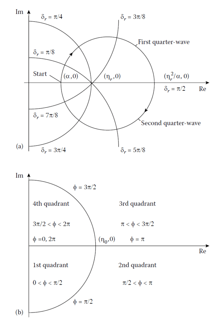
(a) Admittance Locus of a Single Dielectric Film
The locus is a circle centered on the real axis and described in a clockwise direction. The film has a characteristic admittance \( Y \) and is deposited over a substrate or structure with a real admittance \( \alpha \).
Key property: The product of the admittances of the two points of intersection of the locus with the real axis is always \( Y^2 \), the square of the characteristic admittance of the film. The diagram also includes equi-phase-thickness contours, showing lines corresponding to equal phase thickness \(( \delta )\) for the film. These contours help to visualize the change in phase as the film thickness varies.
(b) Contours of Constant Phase Shift on Reflection \(( \phi )\)
Contours of constant phase shift \(( \phi )\) can be added to the admittance diagram. These contours are all circles with centers on the imaginary axis and pass through the point on the real axis corresponding to the admittance \( \eta_0 \) of the incident medium. The four most important contours correspond to phase shifts of: \( 0 \), \( \pi/2 \), \( \pi \), \( 3\pi/2 \). These contours are represented by: Portions of the real axis. A circle centered on the origin that passes through the point \( \eta_0 \). The diagram indicates these contours, and the regions corresponding to the four quadrants of \( \phi \) are marked accordingly.
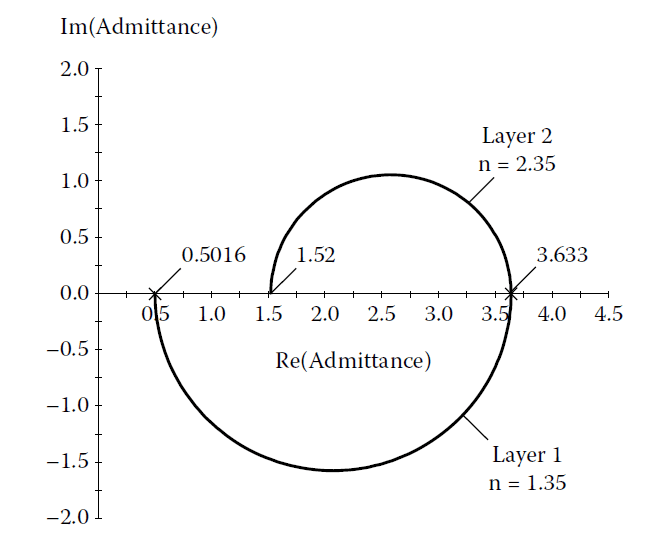
This figure depicts the admittance locus of the multilayer coating configuration: Air | LH | Glass. \( L \): A quarter-wave layer with a refractive index of 1.35. \( H \): A quarter-wave layer with a refractive index of 2.35. Air: Index \( n = 1.00 \). Glass: Index \( n = 1.52 \).
Key Observations:
The starting admittance is \( \eta = 1.52 \), corresponding to the admittance of the glass substrate. The first layer \(H\) traces a semicircular locus on the admittance diagram as it is deposited, ending at \( Y = \frac{2.35^2}{1.52} = 3.633 \) on the real axis. The second layer \(L\) begins at this endpoint and traces another semicircular locus, ending at \( Y = \frac{1.35^2}{3.633} = 0.5016 \) on the real axis.
Similarity:
The admittance diagram for this coating closely resembles Figure 3.12, highlighting the consistency in the shape of the locus for such multilayer designs.

Metal Properties: The metal has a complex refractive index \( n – ik = 2 – i3 \).
Starting Points:
1.00: Represents air as the incident medium (external reflectance locus).
1.52: Represents glass as the incident medium (internal reflectance locus).
Key Observations:
Initial Direction: The loci start in the lower-right direction on the admittance diagram.
Behavior of Reflectance: Internal Reflectance (Air as Substrate, Glass as Incident Medium): Reflectance initially falls as the metal film begins to deposit. Reflectance later rises, creating a characteristic curve.
External Reflectance (Glass as Substrate, Air as Incident Medium): Reflectance always increases, even for very thin layers. This behavior is due to the different starting points and how the loci evolve with increasing film thickness.
End Point of Loci: For very thick metal layers, the loci terminate at the point \( 2 – i3 \), corresponding to the bulk material’s optical admittance. At this stage, the film becomes optically indistinguishable from the bulk metal.
Comparison of the Two Loci: The left locus (internal reflectance) has a distinct dip at the start, indicating a drop in reflectance before increasing. The right locus (external reflectance) shows a steady increase in reflectance, highlighting the difference in reflectance behavior depending on the arrangement of the substrate and incident medium.
3. Electric Field and Losses in the Admittance Diagram
The optical properties of any material are determined largely by the electrons and their interaction with electromagnetic disturbances. Any optical material is made up of atoms or molecules consisting of heavy positively charged masses surrounded by negatively charged electrons.
These electrons are light and mobile compared with the heavy positively charged nuclei. An electric field can exert a force on a charged particle even while it is stationary, but a magnetic field can interact only when the charged particle moves, and for any significant interaction, the particle must be moving at an appreciable fraction of the speed of light.
At the very high frequencies of optical waves, the magnetic interaction is virtually zero. We have already used the fact that the relative permeability is unity in setting up the basic theory. The interaction between light and a material is, therefore, entirely through the electric field. Where the electric field amplitude is high, the potential for interaction is high.
When thin-film optical coatings are illuminated by light, standing wave patterns form that can exhibit considerable variations in electric field amplitude both in terms of wavelength and in terms of position within the coating. The admittance diagram permits a simple technique for assessing these amplitude variations and from them deductions about losses can be made, sometimes with surprising results.
In this discussion, we limit ourselves to normal incidence. Oblique incidence represents only a very slight extension.
Matrix Expression
The basic matrix technique for the calculation of the properties of an optical coating actually contains already the electric field and so only a slight modification is required to extract it. The matrix expression, with the usual meaning for the symbols, is:
\[ \begin{bmatrix} B \\ C \end{bmatrix} = \begin{bmatrix} \cos \delta & i \sin \delta / y \\
i y \sin \delta & \cos \delta \end{bmatrix} \begin{bmatrix} E \\ H \end{bmatrix} \]
Here, \(B\) and \(C\), and the corresponding terms in the other column matrix, are normalized total tangential electric and magnetic fields. The admittances, too, are normalized so that they are in free-space units rather than SI units. The first thing we do, therefore, is to restore the expressions to their fundamental form:
\[ \begin{bmatrix} E \\ H \end{bmatrix} = \begin{bmatrix} \cos \delta & i \sin \delta / y \\ i y \sin \delta & \cos \delta \end{bmatrix} \begin{bmatrix} E \\ H \end{bmatrix} \]
Here \(y\) is in free-space units and so to change it to SI units we must write \(y = (n – ik)Y\), where \(Y\) is the admittance of free space. \(E\) and \(H\) indicate the complex tangential amplitudes that include the relative phase.
Absolute Tangential Electric Field Amplitude
To have absolute values for the total tangential electric field amplitude through the multilayer, it remains simply to give an absolute value to one of the \(E\)’s. This can be done in a number of ways.
The easiest is to put a value on the final tangential component at the emergent interface, that is, the interface with the substrate. This is related to the incident irradiance through the transmittance. If the incident irradiance is \(I_{\text{inc}}\), then:
\[
\frac{1}{2} \text{Re}(E_{\text{exit}} \cdot H_{\text{exit}}^*) = T \cdot I_{\text{inc}}
\]
but \(H_{\text{exit}} = y_{\text{exit}} E_{\text{exit}}\), and so:
\[
\frac{1}{2} \text{Re}(E_{\text{exit}} \cdot y_{\text{exit}}^* E_{\text{exit}}^*) = T \cdot I_{\text{inc}}
\]
Now \(E \cdot E^* = E^2\), giving, with a little manipulation:
\[
E_{\text{exit}} = \sqrt{\frac{2 T I_{\text{inc}}}{\text{Re}(y_{\text{exit}})}}
\]
where \(y_{\text{exit}}\) must be in SI units, that is, siemens.
Electric Field and Admittance Relationship
If the multilayer system is completely free of absorption, then there is a simple connection between the variation of admittance through the multilayer, which is the quantity we plot in the admittance diagram, and the electric field amplitude.
The admittance at any point in the multilayer is simply the ratio of the total tangential magnetic and electric fields. These total tangential fields also yield the total net irradiance transmitted by the multilayer. Since this multilayer is free of losses, the transmitted irradiance is constant through the multilayer. Putting all this together gives:
\[
|E|^2 \propto \frac{1}{\text{Re}(Y)}
\]
Contours of constant electric field are therefore lines normal to the real axis in the admittance diagram. If we put \(Y\) in free-space units, then:
\[
|E| = \sqrt{\frac{27.46 \, \text{V/m} \cdot T \cdot I_{\text{inc}}}{\text{Re}(Y)}}
\]
Lines of constant electric field amplitude for dielectric materials in the admittance diagram.
The figures are in volt/meter if the transmitted irradiance is 1 watt/square meter.
Absorption in Thin Layers
For a very thin slice of absorbing material embedded in a multilayer, the result is contained in the expression:
\[ \begin{bmatrix} E’ \\ H’ \end{bmatrix} = \begin{bmatrix} \cos(\delta) & i \sin(\delta) / y \\
i y \sin(\delta) & \cos(\delta) \end{bmatrix} \begin{bmatrix} E \\ H \end{bmatrix} \]
where \( \delta = \frac{2 \pi}{\lambda}(n – ik)d \). Let the layer be extremely thin. Since the layer is absorbing:
\[
\delta = \alpha – i \beta
\]
Substituting this, the absorbed irradiance is:
\[
I_{\text{absorbed}} = \frac{4 \pi n k d}{\lambda} \cdot \frac{|E|^2}{\text{Re}(Y)}
\]
Potential Transmittance and Absorption
The potential transmittance of any element of a coating system is defined as the ratio of the output to the net input irradiances, where the input is the net irradiance rather than the incident. For a very thin layer:
\[
\psi = 1 – \frac{4 \pi n k d}{\lambda \cdot \text{Re}(Y)}
\]
Total Absorption in Multilayers
If the absorption is distributed through the layer, the total absorption can be expressed as the sum of individual contributions:
\[
A = A_1 + A_2 + A_3 + \dots
\]
or, in integral form:
\[
A = \int \frac{2 n k}{\text{Re}(Y)} d \delta
\]
4. The Vector Method
The vector method is a valuable technique, especially in design work associated with antireflection coatings. Two primary assumptions are involved:
- No Absorption: There is no absorption in the layers, meaning \( N_r = n_r \) and \( k_r = 0 \).
- Single Reflection per Interface: The behavior of a multilayer is determined by considering only one reflection of the incident wave at each interface.
While this method can introduce errors in cases where the overall reflectance of the multilayer is high, these errors are usually negligible in most antireflection coatings.
Amplitude Reflection Coefficient
The amplitude reflection coefficient at each interface is given by:
\[
\rho = \frac{n_r – n_{r-1}}{n_r + n_{r-1}}
\]
This coefficient may be positive or negative depending on the relative magnitudes of \( n_{r-1} ) and ( n_r \).
Phase Thickness of Layers
The phase thickness of the \( r \)-th layer is given by:
\[
\delta_r = \frac{2 \pi n_r d_r}{\lambda}
\]
Here:
- A quarter-wave optical thickness corresponds to \( 90^\circ \),
- A half-wave corresponds to \( 180^\circ \).
Resultant Reflection Coefficient
The resultant amplitude reflection coefficient is represented as the vector sum of the coefficients for each interface. Each coefficient is associated with the phase lag caused by the wave’s passage from the front surface to the interface and back to the front surface.
Vector Representation
The sum of the reflection coefficients can be found either:
- Analytically, by directly summing the vectors with their respective phase angles, or
- Graphically, which is more practical.
The angles between successive vectors are \( 2\delta_1, 2\delta_2, 2\delta_3, \dots \).
Calculation Simplification
When the optical thicknesses of the layers are expressed in terms of quarter-wave optical thicknesses at a reference wavelength \( \lambda_0 \), the value of \( \delta_r \) at a wavelength \( \lambda \) is:
\[
\delta_r = 90^\circ \cdot t_r \cdot \frac{\lambda_0}{\lambda}
\]
where \( t_r \) is the thickness of the \( r \)-th layer in quarter-waves at \( \lambda_0 \).
Vector Diagram Construction
- To construct the vector diagram:
- Plot each vector with its direction on a polar diagram.
- Transfer these vectors to a vector polygon.
This step-by-step plotting helps avoid confusion, particularly when dealing with negative reflectances.
Reflectance Calculation
The resultant vector in the polygon represents the amplitude reflection coefficient. Its length must be squared to calculate the reflectance:
\[
R = |\rho|^2
\]
Illustrative Example
A typical arrangement is shown in Figure 3.5:
- The vectors corresponding to reflection coefficients at different interfaces are plotted in sequence.
- The resultant vector is obtained as the sum of these vectors.
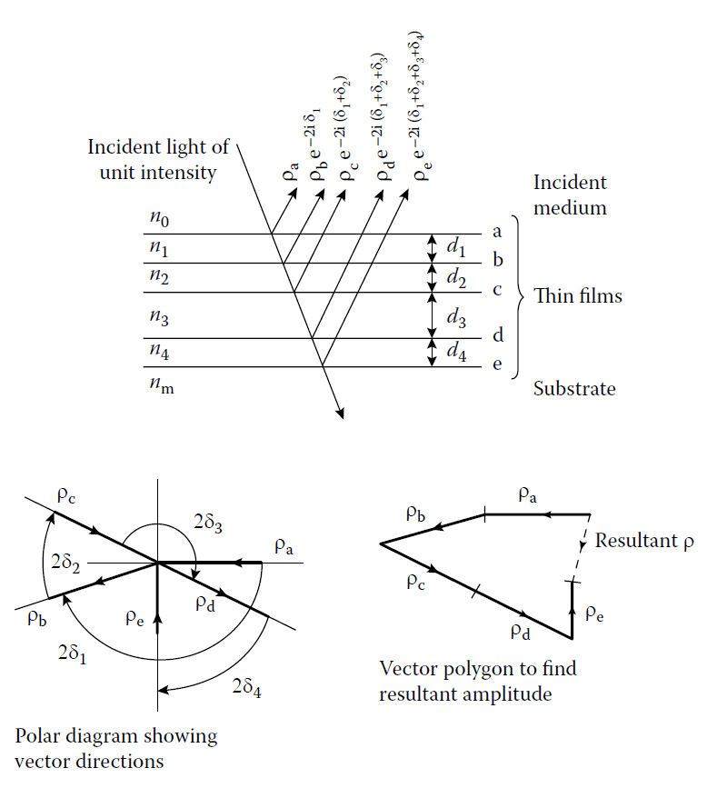
The Vector Method Illustration
The vector method is demonstrated in Figure 3.5, where the reflection coefficients \(( \rho )\) and phase lags \(( \delta )\) of the multilayer structure are represented as vectors.
Lengths of Vectors
The lengths of the reflection coefficient vectors for each layer are determined by the equations:
\[
\rho_a = \frac{n_0 – n_1}{n_0 + n_1}, \quad \delta_1 = \frac{2 \pi n_1 d_1}{\lambda}
\]
\[
\rho_b = \frac{n_1 – n_2}{n_1 + n_2}, \quad \delta_2 = \frac{2 \pi n_2 d_2}{\lambda}
\]
\[
\rho_c = \frac{n_2 – n_3}{n_2 + n_3}, \quad \delta_3 = \frac{2 \pi n_3 d_3}{\lambda}
\]
Important Notes on Signs
Signs of Reflection Coefficients: The sign of each vector’s length is critical and must be included in calculations. In Figure 3.5, the vectors \( \rho_a, \rho_c, \) and \( \rho_e \) are shown as having negative signs.
Phase Lags: The angles between successive vectors correspond to phase lags. The sense of all angles in the polar diagram \(( \delta_1, \delta_2, \delta_3, \dots )\) is negative.
Resultant Reflection Coefficient
The resultant reflection coefficient \(( \rho )\) is calculated as the vector sum of all reflection coefficients, including their respective phase shifts:
\[
\rho = \rho_a + \rho_b \exp(-i\delta_1) + \rho_c \exp(-i(\delta_1 + \delta_2)) + \rho_d \exp(-i(\delta_1 + \delta_2 + \delta_3)) + \dots
\]
Where:
\( \rho_a, \rho_b, \rho_c, \dots \) are the reflection coefficients,
\( \delta_1, \delta_2, \delta_3, \dots \) are the phase shifts introduced by the layers.
Vector Diagram Construction
Plot Vectors: Start by plotting each reflection coefficient as a vector with its corresponding length and angle in the polar diagram.
Add Vectors Sequentially: Successively add the vectors to determine the resultant reflection coefficient \( \rho \).
This method provides a graphical and intuitive way to calculate and visualize the reflectance of a multilayer structure, especially for antireflection coatings.
5. The Herpin Index
The Herpin Index is a critical concept in the design and analysis of optical filters, particularly edge filters and antireflection coatings. This section provides an overview of its utility and foundational principles.
Definition and Importance
- Symmetrical Matrix Replacement: Any symmetrical product of three thin-film matrices can be mathematically replaced by a single matrix. This matrix is equivalent to that of a single thin film with:
- Equivalent thickness, and
- Equivalent optical admittance.
- Mathematical, Not Physical Equivalence: While this equivalence is mathematical, not physical, it significantly simplifies analysis and provides insights into the properties of complex multilayer designs.
Applications
- Filter Design:
- The Herpin Index simplifies the analysis of many filter designs.
- Filters can often be split into symmetrical combinations, which can then be analyzed as single layers using the Herpin Index.
- Intermediate Index Replacement:
- Layers requiring intermediate refractive indices (often unavailable or impractical) can be substituted with symmetrical combinations of high- and low-index materials.
- This technique is particularly useful for antireflection coatings, reducing the total number of materials needed for the structure.
Terminology
- Herpin Index: The equivalent optical admittance derived from the replacement of a symmetrical combination of layers.
- Epstein Period: A symmetrical combination of high- and low-index materials that serves as a substitute for a layer of intermediate refractive index.
Origins and Historical Context
- Herpin Index: Named after the originator of this concept.
- Epstein Period: Named after the author of pivotal early papers applying the concept to filter design.
By leveraging the Herpin Index and Epstein Period, designers can efficiently analyze and construct complex optical coatings while optimizing material usage and performance.
6. Alternative Method of Calculation
The success of the vector method prompts one to ask whether it can be made more accurate by considering second and subsequent reflections at the various boundaries instead of just one. In fact, an alternative solution of the thin-film problem can be obtained in this way, and this was the earlier way of formulating film properties dating back to Poisson.
It is simpler to consider normal incidence only. The expressions can be adapted for non-normal incidence quite simply when the materials are transparent and with some difficulty when they are absorbing. We consider first the case of a single film. Figure 3.6 defines the various parameters.
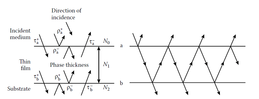
Parameters in the multiple beam summation.
Resultant Amplitude Reflection Coefficient
The resultant amplitude reflection coefficient is given by:
\[
\rho_+ = \rho_a + \tau_a^+ \rho_b^+ \tau_a^- e^{2i\delta_a} + \tau_a^+ \rho_b^+ \rho_a^- \rho_b^- \tau_a^- e^{4i\delta_a} + \cdots
\]
This reduces to:
\[
\rho_+ = \frac{\rho_a + \rho_b^+ e^{2i\delta_a}}{1 + \rho_a^- \rho_b^+ e^{2i\delta_a}}
\tag{3.14}
\]
Resultant Amplitude Transmission Coefficient
Similarly, the transmission coefficient is:
\[
\tau_+ = \tau_a^+ + \tau_a^+ \rho_b^+ \tau_b^- e^{i\delta_a} + \tau_a^+ \rho_b^+ \rho_a^- \tau_b^- e^{3i\delta_a} – \cdots
\]
This simplifies to:
\[
\tau_+ = \frac{\tau_a^+ \tau_b^+ e^{i\delta_a}}{1 + \rho_a^- \rho_b^+ e^{2i\delta_a}}
\tag{3.15}
\]
Iterative Calculations for Multilayer Systems
For assemblies of more than one film, these expressions can be applied successively:
- Start with the final two interfaces and calculate the resultant coefficients \(( \rho_+ \) and \( \tau_+ )\).
- Replace these interfaces with a single equivalent interface.
- Proceed to the next interface, iterating until all layers are considered.
Converting to Reflectance and Transmittance
The resultant amplitude coefficients \(( \rho_+ \) and \( \tau_+ )\) can be converted into reflectance \(( R )\) and transmittance \(( T )\) using the relations:
\[
R = |\rho_+|^2
\]
\[
T = \frac{| \tau_+ |^2 n_2}{n_0}
\]
where \( n_0 \) and \( n_2 \) are the refractive indices of the incident and exit media, respectively. These expressions are meaningful only if the incident medium is transparent, so \( N_0 = n_0 \).
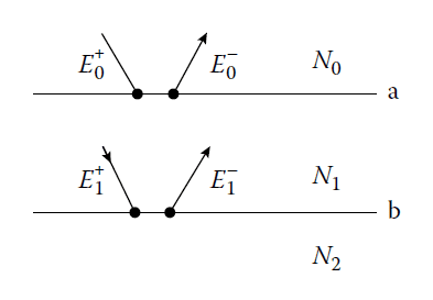
Matrix Representation
The electric field amplitudes in medium 0 \(( E_0^+ \) and \( E_0^- )\) at interface \( a \) can be expressed in terms of the field amplitudes in medium 1 \(( E_1^+ \) and \( E_1^- )\) at interface \( b \) (see Figure 3.7):
\[ \begin{bmatrix} E_0^+ \\ E_0^- \end{bmatrix} = \begin{bmatrix} \tau_a^+ & \rho_a^+ e^{i\delta_a} \\
\rho_a^- e^{-i\delta_a} & \tau_a^- \end{bmatrix} \begin{bmatrix} E_1^+ \\ E_1^- \end{bmatrix} \tag{3.16} \]
For the second interface:
\[ \begin{bmatrix} E_1^+ \\ E_1^- \end{bmatrix} = \begin{bmatrix} \tau_b^+ & \rho_b^+ \\ \rho_b^- & \tau_b^- \end{bmatrix} \begin{bmatrix} E_2^+ \\ 0 \end{bmatrix} \tag{3.17} \]
Absorbing Layers
If absorption is included, the same formulas apply, but the coefficients \( \rho \), \( \tau \), and \( \delta \) become complex. This allows the method to handle absorbing materials, though it increases computational complexity.
The positive- and negative-going waves at the two interfaces.
Key Points
- When adding layers to an existing multilayer structure, the reflection and transmission coefficients for both the new interface and the previously final interface must be recalculated.
- These recalculations ensure that the method accurately accounts for changes in optical properties due to additional layers.
This alternative method provides a robust way to analyze multilayer systems, extending the simpler vector approach to handle more complex scenarios.
7. Smith’s Method of Multilayer Design
In 1958, Smith, then of the University of Reading, published a useful design method based on Equation (3.15). The technique is also known as the method of effective interfaces. It consists of choosing any layer in the multilayer and then considering multiple reflections within it, where the reflection and transmission coefficients at its boundaries are the resultant coefficients of the complete structures on either side.
The method of summing multiple beams is, of course, quite old, but the novel feature of Smith’s technique is how it is applied. Although the technique was principally concerned with dielectric multilayers, it can be extended to deal with absorbing layers. As before, this derivation is limited to normal incidence. For transparent layers, the expressions can be extended to oblique incidence with relative ease, though absorbing layers introduce additional complexity.
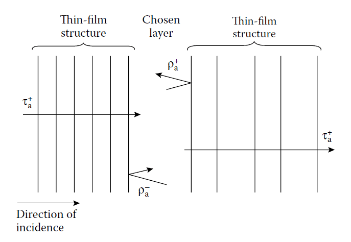
The quantities associated with the effective interfaces in Smith’s technique.
Key Parameters
The notation is illustrated in Figure 3.8. From Equation (3.15):
\[
\tau_+ = \frac{\tau_a^+ \tau_b^+ e^{i\delta_a}}{1 + \rho_a^- \rho_b^+ e^{2i\delta_a}}
\]
where:
\[
\delta = \frac{2\pi N d}{\lambda}
\]
Layer Optical Thickness
The refractive index \( N = n – ik \), so \( \delta \) can be written as:
\[
\delta = \frac{2\pi (n – ik) d}{\lambda} = \alpha + i\beta
\]
with:
\[
e^{-i\delta} = e^{-\beta} e^{-i\alpha}
\]
Here:
- \( \alpha = \frac{2\pi n d}{\lambda} \): phase thickness
- \( \beta = \frac{2\pi k d}{\lambda} \): extinction coefficient
Transmittance
The transmittance \( T \) is given by:
\[
T = \frac{n_m}{n_0} \tau_+ \tau_+^*
\]
where \( n_0 \) and \( n_m \) are the refractive indices of the incident and exit media, respectively. Substituting for \( \tau_+ \) and simplifying:
\[
T = \frac{n_m}{n_0} \frac{\tau_a^+ \tau_a^{+} \tau_b^+ \tau_b^{+} e^{-\beta} e^{-2\beta}}{|1 – \rho_a^- \rho_b^+ e^{-2\beta} e^{i\alpha}|^2}
\]
This becomes:
\[
T = \frac{n_m}{n_0} \frac{\tau_a^+ \tau_b^+ e^{-\beta} \cos(\phi_a + \phi_b + \alpha)}{1 – |\rho_a^- \rho_b^+|^2 e^{-4\beta}}
\]
Simplified Case: No Absorption
If the chosen layer has no absorption \(( \beta = 0 )\), the transmittance simplifies further:
\[
T = \frac{n_m}{n_0} \frac{\tau_a^+ \tau_b^+}{1 – |\rho_a^- \rho_b^+|^2}
\]
and:
\[
T = \frac{\tau_a^+ \tau_b^+}{1 – |\rho_a^- \rho_b^+|^2} \times \left( 1 – R_a^- \right) \left( 1 – R_b^+ \right)
\]
Revised Expression
The more commonly quoted version of this transmittance is:
\[
T = T_a T_b \left( 1 – R_a^- R_b^+ \right) \sin^2 \left( \phi_a + \phi_b + \frac{2\pi nd}{\lambda} \right)
\tag{3.20}
\]
Applications
This method is especially useful for:
- Filter design: Provides insights into the properties of specific types of filters.
- Layer influence: Isolates layers or layer combinations to examine their effect on filter performance.
However, for determining the performance of a given multilayer, the matrix method remains the most straightforward and efficient approach.
Smith’s original paper includes many examples of this approach and is a valuable resource for further study.
8. The Smith Chart
The Smith Chart is a graphic tool originally devised to simplify calculations involving reflection coefficients and admittances in thin-film systems. Although its use is not emphasized in the remainder of the book, it is included here for its historical significance and utility in understanding multilayer systems. The method depends on three properties of a thin-film structure:
Key Properties
- Continuity of Tangential Fields
The tangential components of \( E \) and \( H \) are continuous across a boundary. Consequently, the equivalent admittance is also continuous. - Phase-Related Reflection Coefficient
Within a thin film (e.g., layer \( q \) in Figure 3.9), the amplitude reflectance \( \rho \) at any plane within the layer is related to the amplitude reflectance \( \rho_m \) at the boundary farthest from the incident wave by:
\[
\rho = \rho_m e^{-2i\delta}
\tag{3.21}
\]
where \( \delta \) is the phase thickness of the layer between the boundary and the plane in question. - Front Surface Reflection Coefficient
The amplitude reflection coefficient \( \rho \) at the front surface of any thin-film assembly is related to its optical admittance \( Y \) by:
\[
\rho = \frac{\eta_0 – Y}{\eta_0 + Y}
\tag{3.22}
\]
where \( \eta_0 \) is the admittance of the incident medium. The ratio \( Y/\eta_0 \) is often called the reduced admittance.
Calculation Procedure Using the Smith Chart
The Smith Chart simplifies the calculation of the amplitude reflection coefficient for a multilayer system. The process involves these steps:
- Boundary Reflection Coefficient
Start with \( \rho_m \), the amplitude reflection coefficient at the boundary of the layer farthest from the incident wave. - Reflection Coefficient Inside the Layer
Calculate the reflection coefficient just inside the boundary \( l \) using:
\[
\rho = \rho_m e^{-2i\delta_q}
\tag{3.23}
\] - Optical Admittance Just Inside the Boundary
Use the reduced admittance relationship:
\[
Y_q = \eta_q \frac{1 + \rho}{1 – \rho}
\tag{3.25}
\] - Optical Admittance on the Incident Side
Because of the continuity of tangential fields, the optical admittance on the incident side of boundary \( l \) is the same as \( Y \) at that point. The reduced admittance is given by:
\[
Y_{q-1} = \frac{\eta_q}{\eta_q – \eta_q^{-1} \cdot Y_q}
\tag{3.26}
\] - Reflection Coefficient on the Incident Side
Finally, calculate the reflection coefficient on the incident side of the boundary:
\[
\rho_l = \frac{Y_{q-1} – \eta_{q-1}}{Y_{q-1} + \eta_{q-1}}
\tag{3.27}
\]
Sequential Application
The reflection coefficient for a multilayer system is found by applying Equations (3.23)–(3.27) successively to each layer, starting from the layer farthest from the incident wave and moving towards it.
The Smith Chart
- The Smith Chart connects values of \( X \) and \( Z \), where:
\[
X = \frac{Z – 1}{Z + 1}
\tag{3.28}
\]
Here, \( Z \) is plotted in polar coordinates, and \( X \) is determined from orthogonal circles on the chart. - To account for phase changes \(( 2\delta_q )\), the chart includes a scale around its perimeter. The point corresponding to \( \rho_m \) is rotated around the chart’s center by the angle \( 2\delta_q \), calibrated in fractions of a wavelength.
Figure 3.10 illustrates the Smith Chart, showing how the relationships between \( X \), \( Z \), and phase angles are visualized.
Figure 3.9
Illustration of the thin-film structure and relevant parameters for applying the Smith Chart. Each layer is identified with its admittance \( \eta \), and \( \rho \) represents the amplitude reflection coefficients at various boundaries. The phase thickness \( \delta \) relates the reflection coefficients inside the layer to those at its boundaries.

Parameters used in the Smith Chart description.
Figure 3.10
The Smith Chart:
- Outer Scale: Represents the phase changes \( 2\delta_q \), measured in fractions of a wavelength.
- Polar Coordinates: Plots \( Z \), with corresponding real and imaginary components of \( X \) determined using the orthogonal circle intersections.
- Application: The reflection coefficient \( \rho_m \) is rotated by \( 2\delta_q \) on the chart to determine the new coefficient.
This tool visually integrates the relationships among reflection coefficients, admittance, and phase changes for multilayer systems.
The Smith Chart offers a graphic approach for solving thin-film problems and, while it is not used extensively here, it remains an insightful tool for understanding and approximating multilayer behavior.
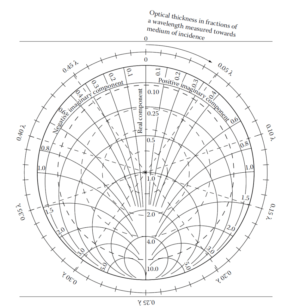
The Smith Chart. Broken circles are circles of constant amplitude reflection coefficient ρ. From
the smallest to the largest they correspond to ρ = 0.2, 0.4, 0.6, 0.8 and 1.0, the outer solid circle.
Solid circles are circles of constant real part and constant imaginary part of the reduced optical
admittance. Note: An optical thickness of 0.25λ corresponds to a phase thickness of 90°.
9. Reflection Circle Diagrams
The Reflection Circle Diagram technique, sometimes referred to as the circle diagram, was initially described by Berning and later developed extensively by Apfel. According to Apfel, Frank Rock originated the method in the mid-1950s. While the appearance of these diagrams resembles that of the Admittance Diagram and the Smith Chart, the underlying concepts differ.
Key Differences
- The Smith Chart slides a reference plane through an existing multilayer structure, plotting the net amplitude reflection coefficient at the plane. The resulting loci exhibit discontinuities when an interface is crossed. Dielectric loci are circles centered at the origin.
- The Circle Diagram assumes the multilayer is being constructed layer by layer. Here, the incident medium remains the same for the entire multilayer. As a result, the loci are continuous, with no discontinuities, and dielectric circles are not centered at the origin.
Equation for Amplitude Reflection Coefficient
The change in the amplitude reflection coefficient upon adding a single layer is given by Equation (3.14):
\[
\rho = \frac{\rho_f^+ + \rho’ e^{-2i\delta}}{1 + \rho_f^+ \rho’ e^{-2i\delta}}
\tag{3.29}
\]
Where:
- \( \rho_f^+ \): Amplitude reflection coefficient at the outer interface (boundary \( f \)).
- \( \rho’ \): Resultant amplitude reflection coefficient at the inner interface, considering the entire structure on that side.
- \( \delta \): Phase thickness of the added layer.
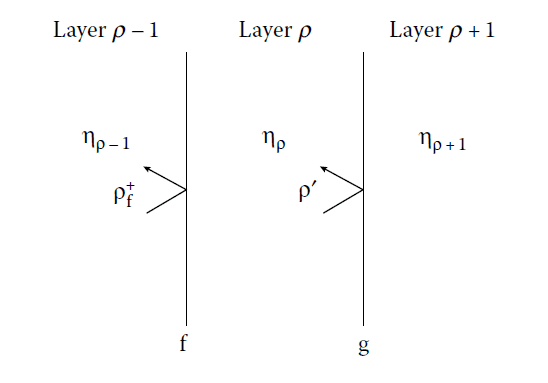
Quantities in the method of reflection circles.
Locus of Reflection Coefficient
The locus of \( \rho \) in the complex plane as \( \delta \) varies can be analyzed as follows:
- Substitute \( \rho = x + iy \) and \( \rho’ e^{-2i\delta} = \alpha + i\beta \), where:
\[
\alpha^2 + \beta^2 = (\rho’)^2
\] - Expanding Equation (3.29), the real \(( x )\) and imaginary \(( y )\) parts of \( \rho \) are:
\[
x_f + y_f = \frac{(x_f – \rho_f^+)(1 – (\rho’)^2) + 2\beta}{1 – (\rho’)^2}
\]
\[
y = \frac{2\rho_f^+ \beta}{1 – (\rho’)^2}
\] - Eliminating \( x_f \) and \( y_f \), the equation simplifies to:
\[
\left(x – \rho_f^+ \frac{1 – (\rho’)^2}{\rho_f^+}\right)^2 + y^2 = \frac{1 – (\rho’)^2}{\rho_f^+}
\]
This is the equation of a circle with:
- Center: \( \frac{(1 – (\rho’)^2)}{\rho_f^+} \)
- Radius: \( \sqrt{1 – (\rho’)^2} \)
A quarter-wave layer traces out a semicircle; a half-wave layer completes the circle.
Example: A Two-Layer System
Consider a substrate of glass \(( n = 1.52 )\) with:
- A quarter-wave layer of zinc sulfide \(( n = 2.35 )\).
- A quarter-wave layer of cryolite \(( n = 1.35 )\).
- Air as the incident medium \(( n = 1.0 )\).
Using Equation (3.29), the terminal points for each layer are calculated:
- First Layer (Zinc Sulfide):
Starting from bare glass in air \(( \rho = -0.2063 )\):
\[
\rho’ = \frac{\rho_f^+ + \rho e^{-2i\delta}}{1 + \rho_f^+ \rho e^{-2i\delta}}
\]
For a quarter-wave layer \(( e^{-2i\delta} = -1 )\):
\[
\rho’ = -0.5683
\] - Second Layer (Cryolite):
Starting from the end of the first layer \(( \rho’ = -0.5683 )\):
\[
\rho_f^+ = -0.1489, \quad \rho’ = -0.4582
\]
The final loci for both layers are shown in Figure 3.12.
Advantages of the Reflection Circle Diagram
- Continuous Loci: Unlike the Smith Chart, the loci are continuous because each layer’s termination serves as the starting point for the next.
- Material Templates: Templates of nested circles for each material simplify diagram construction.
- Compatibility with Smith Chart: Loci can be plotted on the same diagram, even though the techniques differ fundamentally.
Figure 3.12
This figure illustrates the reflection circle loci for the two-layer system:
- Semicircles: Each quarter-wave layer traces a semicircular arc.
- Starting and Terminal Points: Points correspond to the amplitude reflection coefficients at the beginning and end of each layer.
This graphic approach provides an intuitive method for visualizing multilayer reflection properties. Further examples and extended applications, including absorbing layers, are discussed by Apfel.
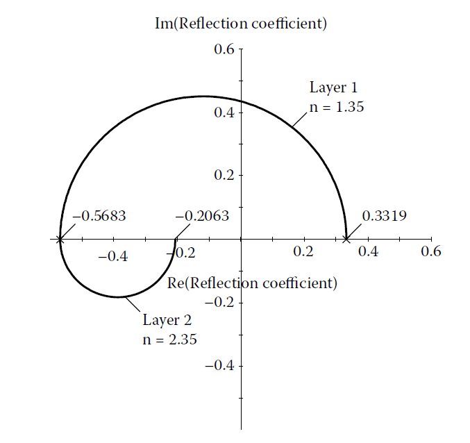
Reflection circles, or amplitude reflection locus, for the coating: Air€ |LH|€ Glass, where L
indicates a quarter-wave of index 1.35, H of 2.35, and the indices of air and glass are 1.00 and
1.52, respectively