Optical thin-film coatings can be created using a variety of deposition techniques. Historically, common methods for producing high-performance multilayer coatings—such as those used in mirrors and filters—have included thermal evaporation, electron-beam (e-beam) evaporation, and ion-assisted e-beam evaporation (IAD).
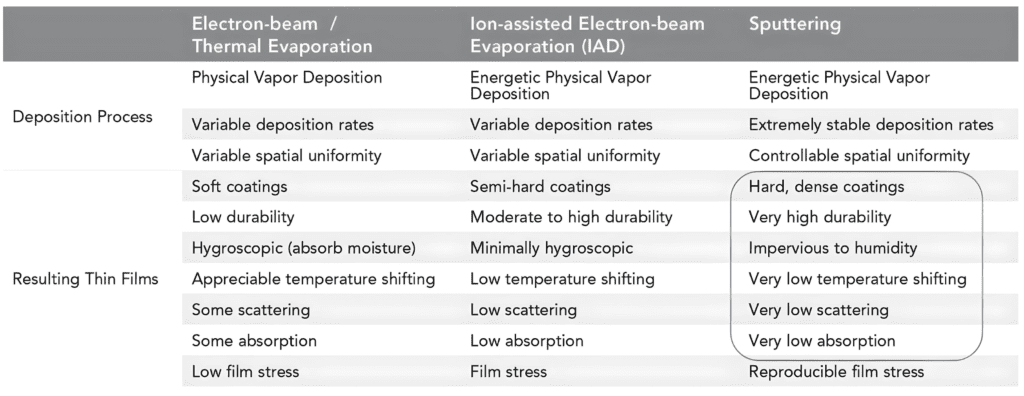
These techniques have been used for decades, but they are not without their challenges. Films produced without ion-assist are known as “soft” coatings because of their porous structure. This porosity leads to significant drawbacks: these coatings are less durable, absorb moisture from the air (causing shifts in optical properties), and are prone to temperature-induced wavelength shifts and increased scattering of light.
By using ion assistance during deposition, IAD coatings achieve greater film density, leading to what are often called “semihard” coatings. These films offer better durability, reduced moisture absorption, and enhanced resistance to temperature fluctuations, but they still don’t fully address the limitations of uniformity and precision when producing complex multilayer filters.
The Ion Beam Sputtering Advantage
In contrast, Notch Optics employs an advanced process known as ion beam sputtering (IBS) for the production of all its optical filters.
IBS is a highly controlled and precise method for depositing thin-film coatings, developed initially for specialized applications in the electronics and magnetic storage industries. However, it was quickly adopted in the optical field because of its superior performance.
Unlike traditional evaporation methods, IBS utilizes a directed ion beam to sputter material from a target onto a substrate, achieving highly dense, durable coatings with exceptional uniformity and thickness control.
Ion Beam Deposition Processes: How It Works
Ion beam sputtering (IBS) is a type of physical vapor deposition (PVD) technique, which is distinct from chemical vapor deposition (CVD). Both methods are used to grow thin films on a substrate, but PVD relies on physical processes, while CVD uses chemical reactions to achieve film growth.
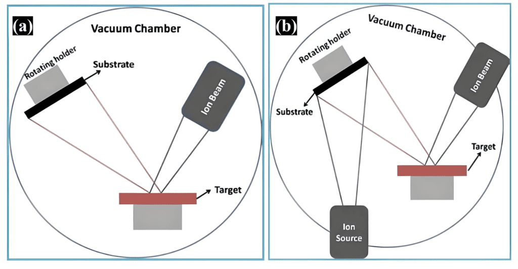
In PVD, thin films are deposited onto a substrate in a vacuum chamber using metallic or dielectric materials. During ion beam deposition (IBD), low-energy ions generated by a broad-beam ion source with high-voltage acceleration are directed at the target material. These ions collide with the target substrate, causing atoms and molecules to be ejected from the target surface.
As these ejected particles are expelled, they begin to condense on the substrate, forming a thin-film layer. This process involves both sputtered atoms from the target material and scattered incident ions bonding tightly to the substrate surface. To further refine and control the IBD process, manufacturers can use a second ion source (often called an ion gun) aimed directly at the substrate to enhance the precision of deposition.
For IBS to work effectively, a deposition system with a high-quality vacuum chamber is essential, ensuring the sputtering and condensation processes occur properly for the thin film’s growth. The size and configuration of IBS systems can vary depending on their application in different industries.

Ion beam sputtering excels where other methods fall short. For example, evaporated coatings often suffer from variability due to the plume of vaporized material, making it challenging to control layer thicknesses across large substrates. This can lead to inconsistent performance in optical components. IBS, on the other hand, produces layers that are incredibly uniform, even over large areas.
The process achieves this by using a focused ion beam to physically eject particles from the target material, which are then deposited onto the substrate with minimal scattering. The result is a coating that is not only denser but also much more durable and less prone to environmental shifts, such as changes in temperature or humidity.

High-Density Thin Films and Surface Morphology
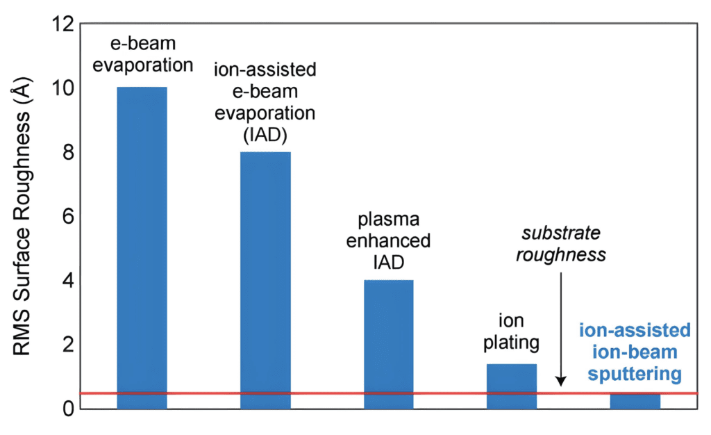
One key advantage of ion beam sputtering is the high packing density of the resulting films. Surface morphology studies using techniques like atomic force microscopy (AFM) reveal that IBS films exhibit minimal surface roughness, closely matching the smoothness of the original substrate.
This is in stark contrast to films produced through e-beam evaporation, which tend to have a rougher surface due to their lower packing density. This high-density structure is what makes IBS coatings “hard” coatings, offering excellent durability and minimal light scattering, which are crucial for high-performance optical filters.

Moreover, the dense nature of IBS films means they are less susceptible to environmental factors. Unlike “soft” coatings, which can absorb water vapor and experience shifts in their optical properties, IBS coatings are stable and reliable under a wide range of conditions, making them ideal for demanding applications like telecommunications, laser optics, and scientific instrumentation.

Ion Beam Sputtering vs. Magnetron Sputtering
While ion beam sputtering (IBS) offers precise control over the chemical and mechanical properties of thin films, it’s not the only sputtering method used in physical vapor deposition (PVD). Magnetron sputtering is another popular PVD technique, though it operates quite differently from IBS.
Magnetron sputtering works by using a magnetic field to confine the target and substrate while an inert gas is fully ionized into plasma between them. Positive ions from the plasma are rapidly accelerated toward the sputtered target, which is electrically biased to help eject material onto the substrate. Magnetron sputtering can be performed at lower pressures, as the magnets help stabilize the plasma and enhance the deposition process.
The major distinction between ion beam sputtering and magnetron sputtering lies in the plasma location. In IBS, the plasma is housed within the ion source, meaning there is no plasma between the target and substrate. This unique setup also allows ion beam sputtering to operate without the need for target biasing, making it suitable for a wider range of materials, including sensitive, conductive, and non-conductive substrates and target materials.
Another key advantage of ion beam sputtering is the level of independent control it offers. Manufacturers can finely tune parameters such as the target sputtering rate, ion energy, angle of incidence, ion current density, and ion flux. This results in a coating that is smooth, dense, and adheres tightly to the substrate.
Advantages and Disadvantages of Ion Beam Sputtering
Ion beam sputtering offers numerous benefits for manufacturers across various industries, including enhanced energy bonding properties, versatility, precision control, and excellent uniformity in coatings.
Energy Bonding
The energy involved in ion beam sputtering is around 100 times higher than in standard vacuum coatings. Even after deposition, the residual kinetic energy helps form a stronger bond, improving the overall quality of the coating.
Uniformity
Ion beam sputtering typically uses a large target surface, which leads to better uniformity in the deposited films. This technique also provides more flexibility in terms of composition and target material options compared to other sputtering methods.
Precise Control
IBS allows for precise manipulation of the ion beam’s focus and scan patterns, along with detailed control over the sputtering rate, ion energy, and current density. This makes it possible to optimize the deposition conditions for specific applications.
Despite its many advantages, ion beam sputtering has certain limitations. For instance, when coating large surfaces that require uniform thickness, IBS might not be ideal due to its relatively low deposition rate. Even when using dual ion beam systems, the limited target area can slow down the process.
Applications of Ion Beam Sputtering and Ion-Assisted Deposition
Ion beam sputtering is particularly valuable for challenging applications that demand precise control over film properties. The ion beam not only aids in deposition but also increases the energy and mobility of atoms before nucleation, improving film quality.
IBS is widely used in industries such as precision optics, semiconductor manufacturing, and nitride film production. Research has shown that bombarding certain films with oxygen (O2+) and argon (Ar+) ions during deposition can lead to significant changes in film properties, such as increased density, improved crystal structure, and reduced water permeability.
Other key applications of IBS include laser bar coating, lenses, and gyroscopes. The precise control that IBS provides allows manufacturers to manipulate surface layers at the atomic level, which is crucial in processes like field electron microscopy, low-energy electron diffraction, and Auger electron spectroscopy.
Another important use of IBS is damage-free cutting of thick films, such as ion beam slope cutting. This technique is particularly useful for optical components like dispersive mirrors, lenses, insulators, and glass substrates.
However, one of the most widespread applications of ion beam sputtering is the deposition of thin films onto substrates of various sizes, including those used in microelectronics. The versatility of the process makes it ideal for both large-scale industrial applications and small-scale precision coatings.
Overcoming Production Challenges with Ion Beam Sputtering
One of the challenges historically associated with ion beam sputtering was the relatively slow deposition rate, which limited its use in high-volume manufacturing. While IBS offered unparalleled precision and performance, it was not seen as a viable option for producing large quantities of filters, especially those with complex designs requiring many layers.
Notch Optics has addressed this issue by developing innovative process technologies that significantly boost deposition rates while maintaining the high level of precision that IBS is known for. These advancements have enabled Notch Optics to scale up production without sacrificing quality.
By optimizing the ion beam’s energy and implementing advanced monitoring and control systems, Notch Optics is able to produce optical coatings with hundreds of precisely controlled layers, even on large substrates. Our proprietary optical monitoring technology allows for real-time adjustments during the coating process, ensuring that each layer meets exacting specifications for thickness and refractive index.
Precision and Performance for Modern Applications
Thanks to its superior control over film thickness and material deposition, ion beam sputtering is the ideal technique for manufacturing complex optical filters with extremely tight performance tolerances. Notch Optics has pioneered the use of IBS for producing filters with hundreds of layers, each only a few nanometers thick, that are tailored for specific optical properties such as wavelength selectivity, polarization control, and reflectivity.
These filters are essential for applications like high-resolution imaging, telecommunications, and laser systems, where even slight variations in coating performance can have a significant impact.
The success of Notch Optics in advancing ion beam sputtering technology has made it possible to deliver high-performance optical coatings that offer unmatched stability, durability, and optical clarity.
By continually refining the IBS process, Notch Optics ensures that its coatings meet the ever-evolving demands of the optical industry, providing reliable solutions for both standard and custom optical components.
Ion beam sputtering is a game-changer for thin-film optical coatings. It offers significant advantages over traditional evaporation techniques, providing higher density, better durability, and greater precision. Notch Optics has taken this technology to the next level, overcoming the limitations of throughput and scale to provide high-volume production of some of the most advanced optical coatings available today.
Final Thoughts
Ion beam sputtering has become an essential tool in modern technology, offering a high level of control and precision in thin-film deposition. Whether used in optics, semiconductors, or microelectronics, IBS provides a way to create smooth, dense films that meet the demanding specifications of today’s advanced applications. Its versatility and accuracy make it one of the leading physical vapor deposition techniques in the industry.
